Liquid crystal display device and manufacturing method of the same

一种液晶显示、设备的技术,应用在晶体管、静态指示器、仪器等方向,能够解决布线高度差、向错等问题,达到降低侧面高度差、降低电阻、粘附性改善的效果

Inactive Publication Date: 2006-09-20
GETNER FOUND L L C
View PDF0 Cites 25 Cited by
  • Summary
  • Abstract
  • Description
  • Claims
  • Application Information

AI Technical Summary

Problems solved by technology

[0007] The present invention provides an LCD device and a manufacturing method thereof, which solve the problems related to the TFT substrate as described above, the problems caused when Cu material is used for wiring, and the disclination due to the height difference of the wiring on the lower layer side defect

Method used


Image

  • Liquid crystal display device and manufacturing method of the same
  • Liquid crystal display device and manufacturing method of the same
  • Liquid crystal display device and manufacturing method of the same

Examples


Embodiment Construction

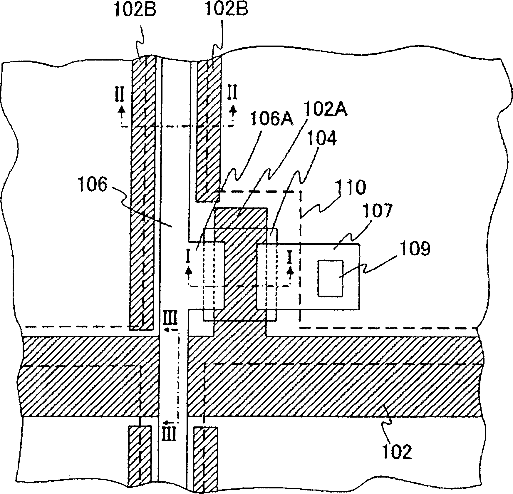
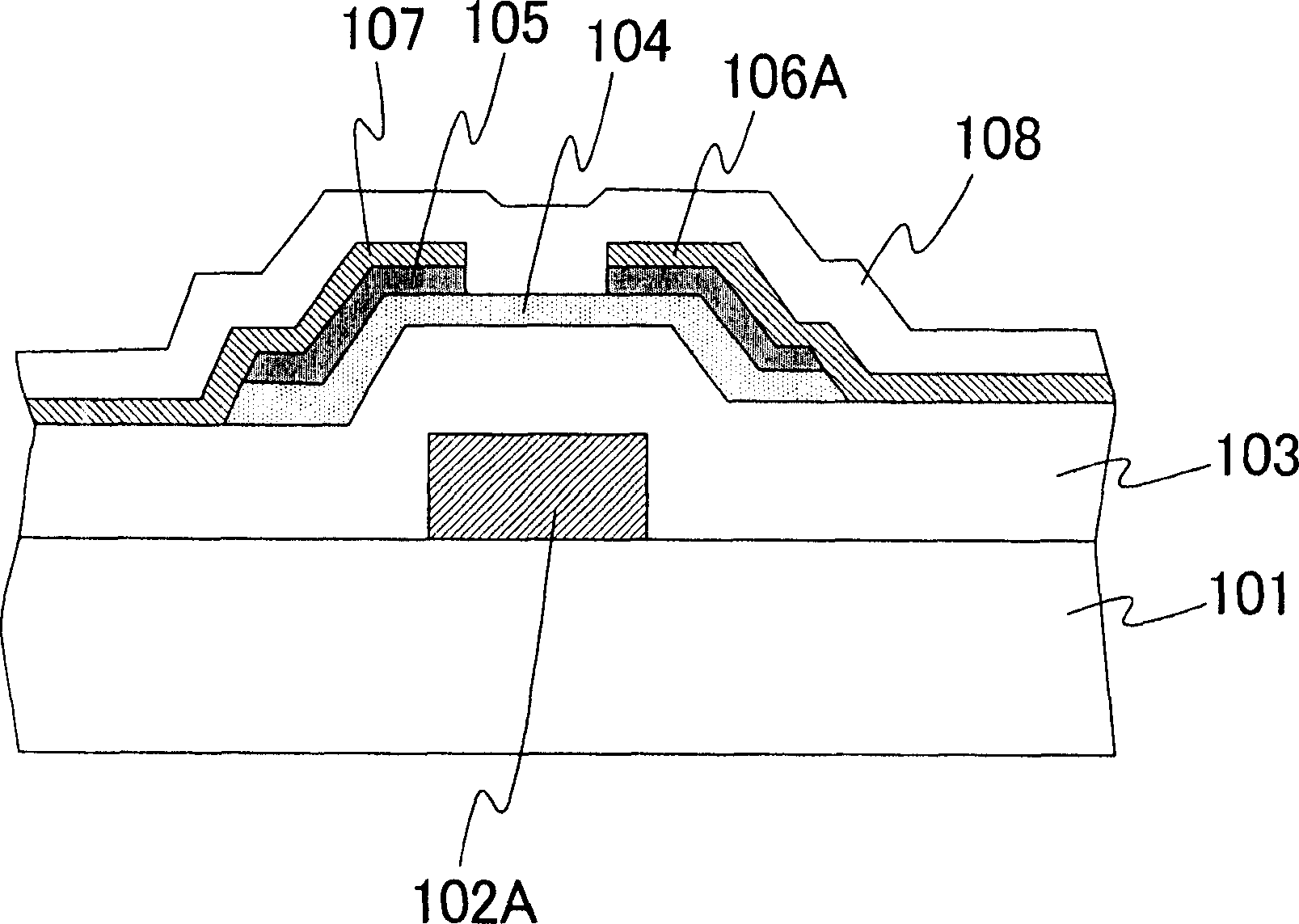
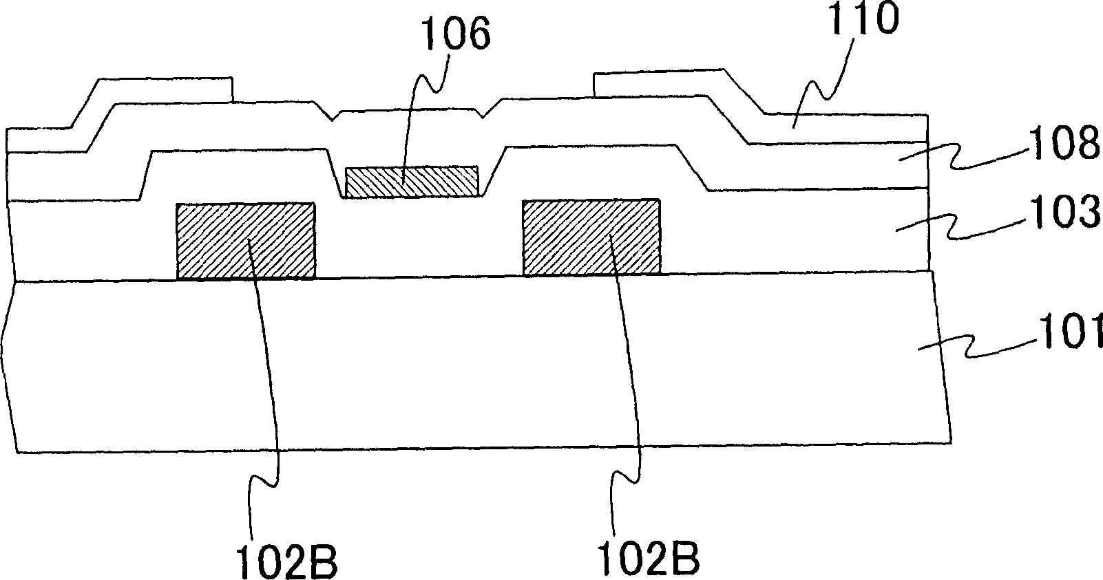
[0024] Embodiments of the LCD device of the present invention will be described with reference to the accompanying drawings. image 3 with Figures 4A to 4C The structure of a TFT substrate as an example of the first substrate for display of the LCD device of the present invention is shown. A gate wiring 2 is formed in a groove on the surface of an insulating substrate 1 made of a glass substrate or a plastic substrate. Incidentally, polycarbonate, polyether sulfone, polyarylate, or the like can be used as the plastic substrate. Drain wiring 6 is formed on insulating substrate 1 so as to be perpendicular to gate wiring 2 . TFTs as switching elements are arranged near the crossing portion between the gate wiring 2 and the drain wiring 6 . The TFT has a gate electrode 2A formed in a trench 12 at the surface of an insulating substrate 1 and a gate insulating film 3 formed on the insulating substrate 1 including the gate electrode 2A, as Figure 4A shown. Gate insulating film ...


PUM


Abstract

An active matrix substrate or TFT substrate is provided with a lower layer wiring with a groove wiring structure covering surroundings of a copper layer with a barrier metal film is formed by forming a groove at an insulating substrate and depositing the barrier metal film and the copper layer in this groove. This groove wiring structure is used for a TFT substrate of a liquid crystal display (LCD) device. It is possible to manufacture an LCD device with large size, high density, a large aperture ratio and in which the disclination defects originating from a different in level of the lower layer wiring and an occurrence of disconnection failures in an upper layer wiring are suppressed.

Description

technical field [0001] The present invention relates to a liquid crystal display (LCD) device and a manufacturing method thereof. In particular, the present invention relates to the structure of a substrate of a display device of an LCD device and a method of manufacturing the same. Background technique [0002] In recent years, active matrix type LCD devices are widely used as displays with high resolution. Such an LCD device has a liquid crystal sandwiched between an active matrix substrate as a first substrate and an opposite substrate as a second substrate. A typical example of an active matrix substrate has a switching element such as a thin film transistor (TFT) at each of a plurality of pixels, and the opposite substrate has a color filter and a black matrix. In this LCD device, the orientation of the liquid crystal molecules varies with the electric field between the electrodes on the active matrix substrate or the TFT substrate and the opposite substrate, or the e...

Claims


Application Information

Patent Timeline
Patent Type & Authority Applications(China)
IPC IPC(8): G02F1/133G02F1/136G02F1/1333H01L29/786
CPCG02F1/136286H01L27/1214G02F1/133305G02F1/136209H01L27/1218G02F2001/136295G02F2001/13629H01L27/124G02F1/13629G02F1/136295G02F1/136
Inventor 安田亨宁铃木圣二
Owner GETNER FOUND L L C
Why Eureka
Try Eureka