Pattern exposure method and apparatus

A graphic exposure and light source technology, which is applied in photolithography exposure devices, microlithography exposure equipment, optics, etc., can solve the problems of low sensitivity and low processing capacity of solder mask

Inactive Publication Date: 2006-09-27
HITACHI SEIKO LTD
View PDF1 Cites 11 Cited by
  • Summary
  • Abstract
  • Description
  • Claims
  • Application Information

AI Technical Summary

Problems solved by technology

However, it is difficult to obtain highly efficient and directional exposure illumination light from a mercury lamp
[0010] In addition, in the case of printed circuit boards, although there is a process of exposing the solder resist film, the sensitivity of the solder resist film is generally low, and the throughput of exposure is low.

Method used


Image

  • Pattern exposure method and apparatus
  • Pattern exposure method and apparatus
  • Pattern exposure method and apparatus

Examples


Embodiment 1

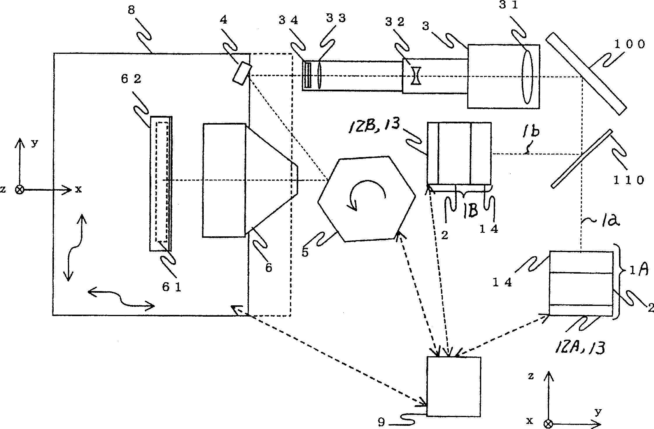
[0030] figure 1 It is a configuration diagram of the maskless exposure apparatus of the first embodiment of the present invention.

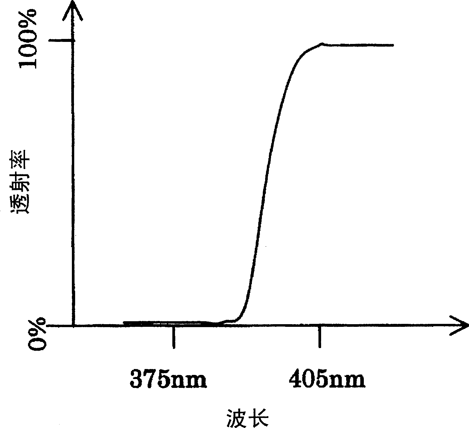
[0031] The light source optical system 1A is composed of a plurality (here, 128) of blue-violet semiconductor lasers 12A that output laser light with a wavelength of 405 nm, etc., and outputs 128 laser beams 1a. In addition, the wavelength of the laser light 1a output from the blue-violet semiconductor laser 12A fluctuates within the range of 405nm±7nm.

[0032] Next, refer to figure 2 The light source optical system 1A will be described in more detail.

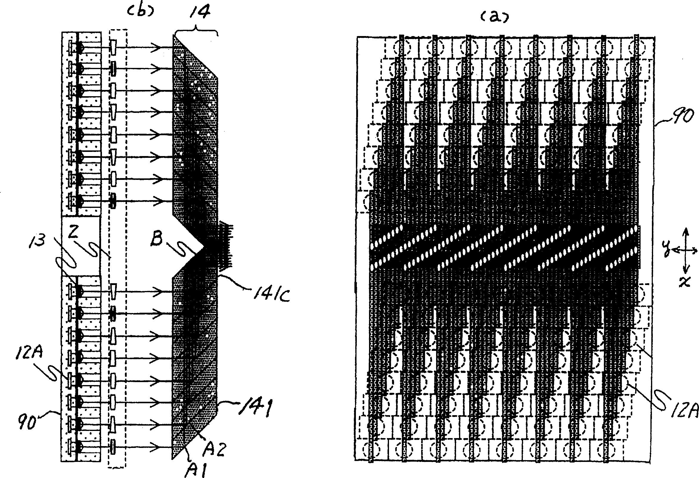
[0033] figure 2 It is a configuration diagram of the light source optical system 1A, (a) is a view viewed from the advancing direction of the laser beam 1a, and (b) is a view viewed from a direction in which the advancing direction of the laser beam 1a is parallel to the paper surface.

[0034] The light source optical system 1A is composed of 128 blue-violet semiconductor lasers 12A arran...

Embodiment 2

[0070] 7 is a configuration diagram of a maskless exposure apparatus according to a second embodiment of the present invention, Figure 8 It is a configuration diagram of the light source optical system 1C, (a) is a view viewed from the advancing direction of the laser light, (b) is a view viewed from the direction in which the advancing direction of the laser light is parallel to the paper surface, and figure 1 , 2 Components with the same or same functions are marked with the same symbols and repeated explanations are omitted.

[0071] In the above-mentioned Embodiment 1, although only the blue-violet semiconductor laser 12A or the ultraviolet semiconductor laser 12B is held on one semiconductor laser holder substrate 90, in this embodiment, 80 blue-violet semiconductor lasers are jointly held on one semiconductor laser holder substrate 90. Semiconductor laser 12A (white circle in the figure) and 48 ultraviolet semiconductor lasers 12B (hatched circle in the figure).

[00...

Embodiment 3

[0077] Figure 9 is a configuration diagram of a maskless exposure apparatus according to a third embodiment of the present invention, and figure 1 , 2 Components with the same or same functions are marked with the same symbols and repeated explanations are omitted.

[0078] A high output semiconductor infrared laser is mounted inside the infrared light source 7 . One side of an optical fiber 71 composed of a plurality of fiber bundles is connected to the infrared light source 7 . The other end portion 72 of the optical fiber 71 is formed by a plurality of optical fibers arranged long in the lateral direction (for example, in a row in the lateral direction), and positioned relatively within the range scanned by the polygon mirror 5 .

[0079] With the above configuration, the infrared light emitted from the semiconductor laser inside the infrared light source 7 enters the optical fiber 71 , exits from the emission end face 72 , and illuminates the range scanned by the polyg...


PUM


Abstract

A maskless exposure method and a maskless exposure apparatus in which maskless exposure can be performed efficiently with high-directivity illumination light, while the exposure efficiency of solder resist can be improved. Blue-violet semiconductor lasers 12 A emitting laser beams 1 a with a wavelength of 405 nm and ultraviolet semiconductor lasers 12 B emitting laser beams 1 b with a wavelength of 375 nm are provided to irradiate a substrate 8 with the laser beams 1 a and 1 b whose optical axes are made coaxial. In this event, one and the same place on the substrate 8 is irradiated with the laser beams 1 a and 1 b a plurality of times. Thus, the variation in intensity of the laser beams 1 a and 1 b is averaged.

Description

technical field [0001] The present invention relates to a pattern exposure method and a pattern exposure device in which a laser is focused and scanned on a substrate to be exposed to draw a pattern, and in particular to a pattern that irradiates a plurality of laser beams output from a plurality of lasers to the base and simultaneously exposes a plurality of locations. Exposure method and device. Background technique [0002] In order to expose patterns on substrates such as printed substrates, TFT substrates for liquid crystal displays, color filter substrates, or plasma displays (hereinafter referred to as substrates), it has been conventional to make a mask as a pattern base, and use the mask Exposure device to expose the substrate. [0003] However, while the size of the substrate has gradually increased in recent years, the time required for designing and manufacturing the substrate has gradually decreased. Furthermore, since it is very difficult to eliminate design ...

Claims


Application Information

Patent Timeline
Patent Type & Authority Applications(China)
IPC IPC(8): G03F7/20H01L21/027
CPCG03F7/70383G03F7/70575G02B26/123G03F7/70466G02B26/12G03F7/70791G02C5/16G02C5/143G02C5/008G02C5/20
Inventor 押田良忠内藤芳达铃木光弘山口刚丸山重信
Owner HITACHI SEIKO LTD
Why Eureka
Try Eureka