Method and device for inspecting a wafer

A measurement device and wafer technology, which is applied in the field of macroscopic defect detection, can solve the problems of inability to adjust, expensive image measurement and image processing, etc., and achieves the effect of reliable identification

Inactive Publication Date: 2006-09-27
LEICA MICROSYSTEMS SEMICON GMBH
View PDF0 Cites 4 Cited by
  • Summary
  • Abstract
  • Description
  • Claims
  • Application Information

AI Technical Summary

Problems solved by technology

To obtain an appropriate pixel resolution, a camera with a higher pixel count is usually used, which makes image determination and image processing more expensive
Furthermore, conventional image determination with a fixed image field is often not optimally adjusted to actual wafer processing conditions

Method used


Image

  • Method and device for inspecting a wafer
  • Method and device for inspecting a wafer
  • Method and device for inspecting a wafer

Examples


Embodiment Construction

[0043] The same reference symbols in the various figures denote identical - or substantially identical - acting elements or groups of elements.

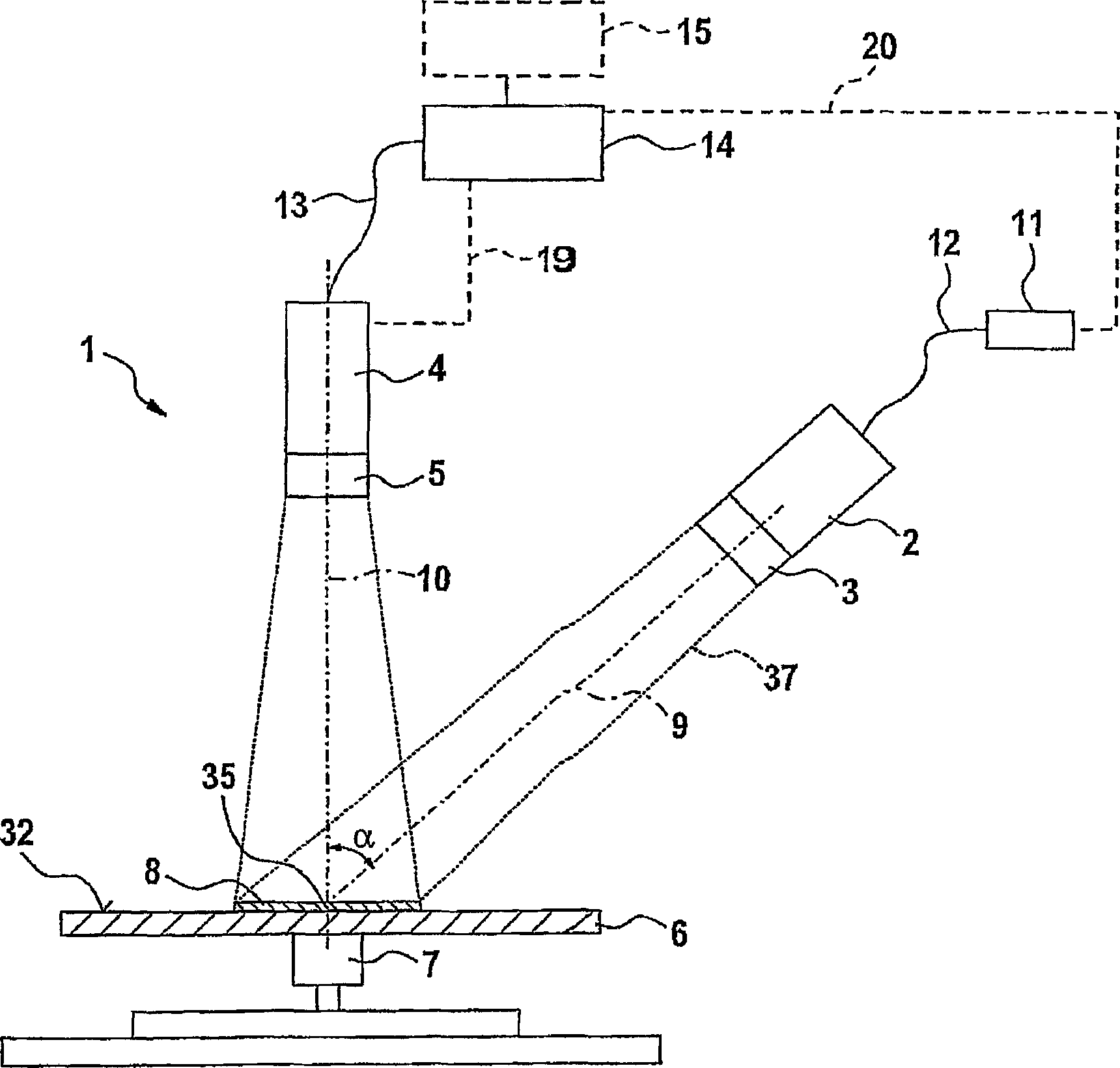
[0044] Such as figure 1 As shown, in the wafer detection device 1, when compared with the prior art, the present invention adopts the following preventive measures: the image measurement device 4 (for example, a column camera or a matrix camera, preferably a CCD- camera) comprising a zoom objective 5 whose focal length can be varied manually or electronically, while the surface 32 of the wafer 6 is continuously imaged in a significant manner in the image measuring device 4 . Alternatively, the distance between the image measuring device 4 and the surface 32 of the wafer 6 can be varied, for example by moving the image measuring device 4 along the imaging axis 10 manually or by an electric motor. After a change in the image distance, this objective 5 has to be precisely readjusted. Another way is to also make the distance between th...


PUM


Abstract

The invention relates to a method and device for inspecting a wafer. The method consists of the following steps: illumination of at least one section of a surface of a wafer; capture of an image of the illuminated section of the surface of the wafer using an image capturing device; determination of at least one image area in the image thus captured; modification of the width of field of the image capturing device on the basis of the at least one image area. Pattern recognition software searches for prominent structures in the captured image in order to determine the image area. The processing speed or resolution of a wafer inspection device can be optimized by modifying the width of field and the image field can be continuously adapted to the shot size of the wafer.

Description

technical field [0001] The present invention relates to a method and apparatus for wafer inspection, and in particular, the present invention relates to a method and apparatus for detecting macro defects with optimized inspection parameters. [0002] figure 1 Wafer inspection setup used to inspect wafers in darkfield configuration is shown. The wafer inspection device 1 comprises a top light-illumination device 2 with an objective lens 3 so that an illumination beam 37 is incident on the surface 32 of the wafer 6 at an angle α along the illumination axis 9 . This illuminating light beam 37 is usually coupled into the top light-illumination device 2 by a separate light source 11 , for example a xenon lamp or a xenon flash lamp, via a light guide 12 . A region 35 is illuminated on the surface 32 of the wafer 6 . [0003] The wafer inspection device 1 additionally comprises an image-determining device 4 with an objective lens 5 , which can be, for example, a matrix camera or a...

Claims


Application Information

Patent Timeline
IPC IPC(8): G01N21/95G02B21/00G02B21/36G06T7/00
CPCG02B21/36G06T7/0004G02B21/0016G01N21/9501G06T2207/30148
Inventor 艾伯特·苛立贺宁·贝克后斯
Owner LEICA MICROSYSTEMS SEMICON GMBH
Why Eureka
Try Eureka