Method for treating semiconductor processing data

A technology for processing data and processing methods, applied in semiconductor/solid-state device manufacturing, comprehensive factory control, comprehensive factory control, etc., can solve problems such as large network load, large data redundancy, large amount of network transmission data, etc., to improve Effects of improving productivity and efficiency

Active Publication Date: 2006-10-25
BEIJING NAURA MICROELECTRONICS EQUIP CO LTD
View PDF0 Cites 16 Cited by
  • Summary
  • Abstract
  • Description
  • Claims
  • Application Information

AI Technical Summary

Problems solved by technology

[0010] For the current completely "passive" processing method, no matter what kind of process data, PMC and TMC will actively send it to CTC every certain time interval, which will inevitably cause a large amount of network transmission data and a large network load , the transmission rate is low, and the data redundancy is large

Method used


Image

  • Method for treating semiconductor processing data
  • Method for treating semiconductor processing data
  • Method for treating semiconductor processing data

Examples


Embodiment Construction

[0028] The following examples are used to illustrate the present invention, but are not intended to limit the scope of the present invention. Those of ordinary skill in the relevant technical field can also make various changes and modifications without departing from the spirit and scope of the present invention. Therefore All equivalent technical solutions also belong to the category of the present invention, and the scope of patent protection of the present invention should be defined by each claim.

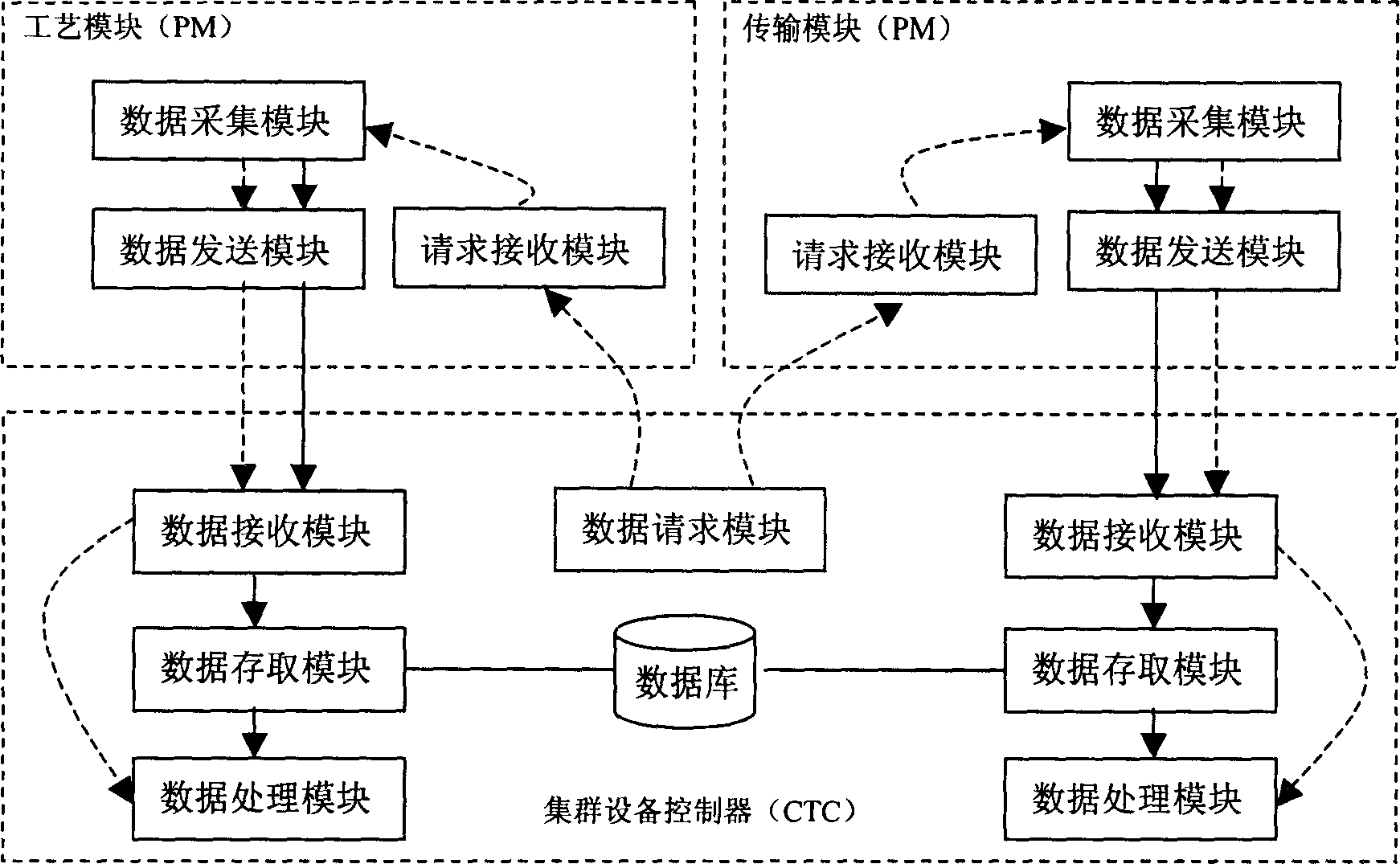
[0029] In order to realize the data processing method of the present invention, a data request module is added in the CTC, and a request receiving module is respectively added in the PMC and the TMC, for the CTC to actively request data from the PMC and / or TMC, and the PMC and / or TMC to respond to the cluster device The controller requests to send data to it, and its functional structure is as follows image 3 shown.

[0030] The system sets different processing modes for rea...


PUM


Abstract

Said method includes 1, dividing semiconductor processing into real time recording data and state monitoring data.2, actively transmitting real time recording data and PMC and / or TMC to CTC at stated time intervals in technology treating processes, or actively querying to PMC and / or TMC at definite-time by CTC. 3, to technology data only meaning equipment momentary state and used for CTC judging setting system working, CTC querying to PMC and / or TMC as in need. When CTC is in no request, PMC or TMC do not transmit these data information to CTC, the network transmission data quantity is greatly reduced, thereby reducing network transmission load and raising network transmission rate.

Description

technical field [0001] The invention relates to a semiconductor processing method, in particular to a processing method for semiconductor cluster equipment processing data. Background technique [0002] The definition of Cluster Tool in the semiconductor standard (SEMI) is: an integrated manufacturing system that is physically connected together and can be used to process different process modules and transmission modules. Each process module and transmission module is controlled by a corresponding controller, and these module controllers are connected into an organic whole through an interface module. [0003] The semiconductor cluster equipment control software system includes three modules: cluster equipment controller (CTC, Cluster Tool Controller), process module controller (PMC, ProcessModule Controller), transmission module controller (TMC, Transport ModuleController), one of the three modules They are connected together through corresponding interface modules. Its ...

Claims


Application Information

Patent Timeline
Patent Type & Authority Applications(China)
IPC IPC(8): G05B19/418G05B23/00H01L21/00
CPCY02P90/02
Inventor 赵昂
Owner BEIJING NAURA MICROELECTRONICS EQUIP CO LTD
Why Eureka
Try Eureka