Non-volatile memory, its production and operation

A non-volatile, manufacturing method technology, applied in semiconductor/solid-state device manufacturing, electric solid-state devices, semiconductor devices, etc., can solve problems such as affecting adjacent memory cells, and achieve the effect of improving reliability

Inactive Publication Date: 2006-11-01
POWERCHIP SEMICON CORP
View PDF0 Cites 5 Cited by
  • Summary
  • Abstract
  • Description
  • Claims
  • Application Information

AI Technical Summary

Problems solved by technology

[0007] In view of this, the purpose of the present invention is to provide a non-volatile memory to solve the existing problem that the voltage applied to a single memory cell will affect the adjacent memory cells during the programming operation.
[0008] Another object of the present invention is to provide the method for manufacturing the above-mentioned non-volatile memory, so as to solve the existing problem that the voltage applied to a single memory cell will affect adjacent memory cells during the programming operation
[0009] Another object of the present invention is to provide the operation method of the above-mentioned non-volatile memory to solve the existing problem that the voltage applied to a single memory cell will affect the adjacent memory cells during the programming operation

Method used


Image

  • Non-volatile memory, its production and operation
  • Non-volatile memory, its production and operation
  • Non-volatile memory, its production and operation

Examples


Embodiment Construction

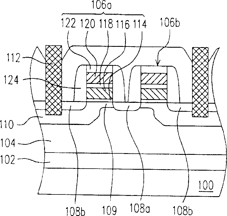
[0060] In the following embodiments, the present invention is described by taking the first conductivity type as n-type doping type and the second conductivity type as p-type doping type. However, those skilled in the art can easily deduce that the doping types of the first conductivity type and the second conductivity type can be exchanged with each other, so the description of the opposite doping types of the following embodiments is omitted. In addition, in the following embodiments, a NOR type non-volatile memory sharing the same auxiliary gate layer is used for illustration.

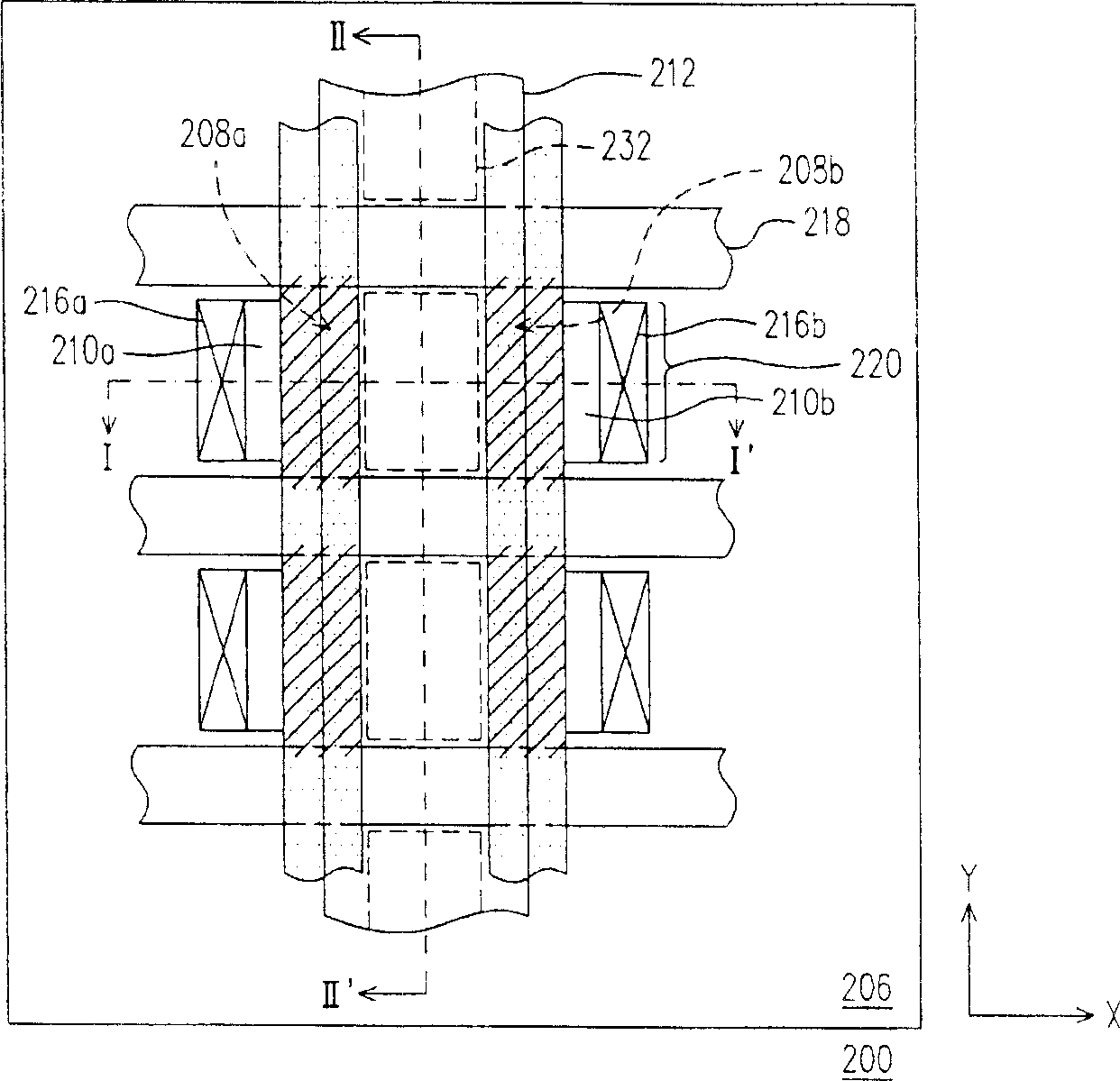
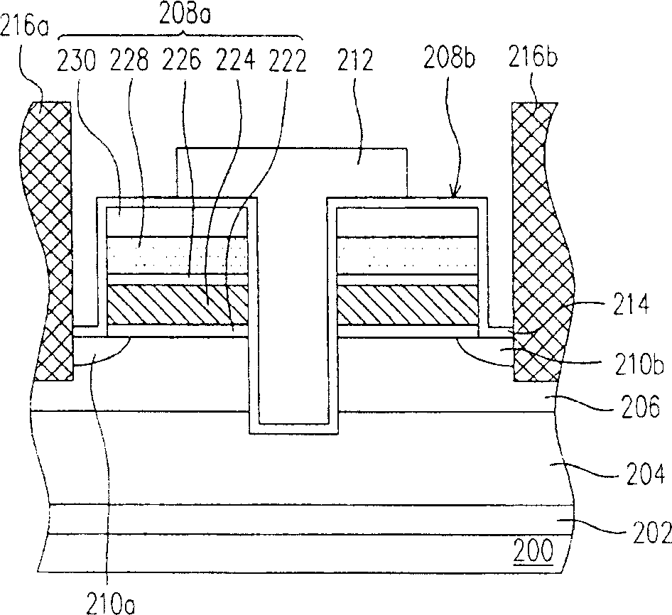
[0061] figure 2 It is a schematic top view illustrating a non-volatile memory according to a preferred embodiment of the present invention. Figure 3A By figure 2 The cross-sectional schematic diagram obtained from the I-I' section (X direction). Figure 3B By figure 2 The schematic cross-sectional view obtained from the II-II' section (Y direction).

[0062] Please also refer to figure 2 ...


PUM


Abstract

The well region of the non-volatile memory cell is formed at a substrate. A shallow well region is formed at said well region. At least two gate stacks are located on the substrate. The drain region is formed in the gate stack proximate the outer edge of said shallow well. The auxiliary gate layer is formed on the substrate between said two gate stacks, and passes through partial substrate. The dielectric layer is formed between said dielectric layer and substrate and between said auxiliary gate layer and gate stacks. The conducting plug is formed on said substrate, and extended down to said shallow well and said drain region therein.

Description

technical field [0001] The present invention relates to a memory element, its manufacturing method and its operating method, in particular to a non-volatile memory, its manufacturing method and its operating method. Background technique [0002] Non-volatile memory has been widely used in personal computers and electronic devices due to its advantages that data can be stored, read, and erased multiple times, and the stored data will not disappear after power failure. a memory element. [0003] A typical non-volatile memory uses doped polysilicon to make a floating gate (Floating Gate) and a control gate (Control Gate). When the non-volatile memory element is programmed or erased, an appropriate voltage is applied to the source region, the drain region, and the control gate to inject electrons into the floating gate, or to remove electrons from the floating gate. Set the gate to pull out. Generally speaking, the charge injection modes commonly used in non-volatile memories...

Claims


Application Information

Patent Timeline
Patent Type & Authority Applications(China)
IPC IPC(8): H01L27/105H01L21/8246H01L21/8247H01L27/115H01L29/788
Inventor 翁伟哲杨青松卓志臣
Owner POWERCHIP SEMICON CORP
Why Eureka
Try Eureka