Semiconductor device

A semiconductor, reverse conduction technology, applied in semiconductor devices, electrical components, circuits, etc., can solve problems such as protection diode damage, achieve the effects of preventing deterioration of withstand voltage, reducing curvature change, and improving withstand voltage characteristics

Inactive Publication Date: 2006-11-01
SANYO ELECTRIC CO LTD
View PDF3 Cites 6 Cited by
  • Summary
  • Abstract
  • Description
  • Claims
  • Application Information

AI Technical Summary

Problems solved by technology

Also, there is a problem of destruction of the protection diode due

Method used


Image

  • Semiconductor device
  • Semiconductor device
  • Semiconductor device

Examples


Embodiment Construction

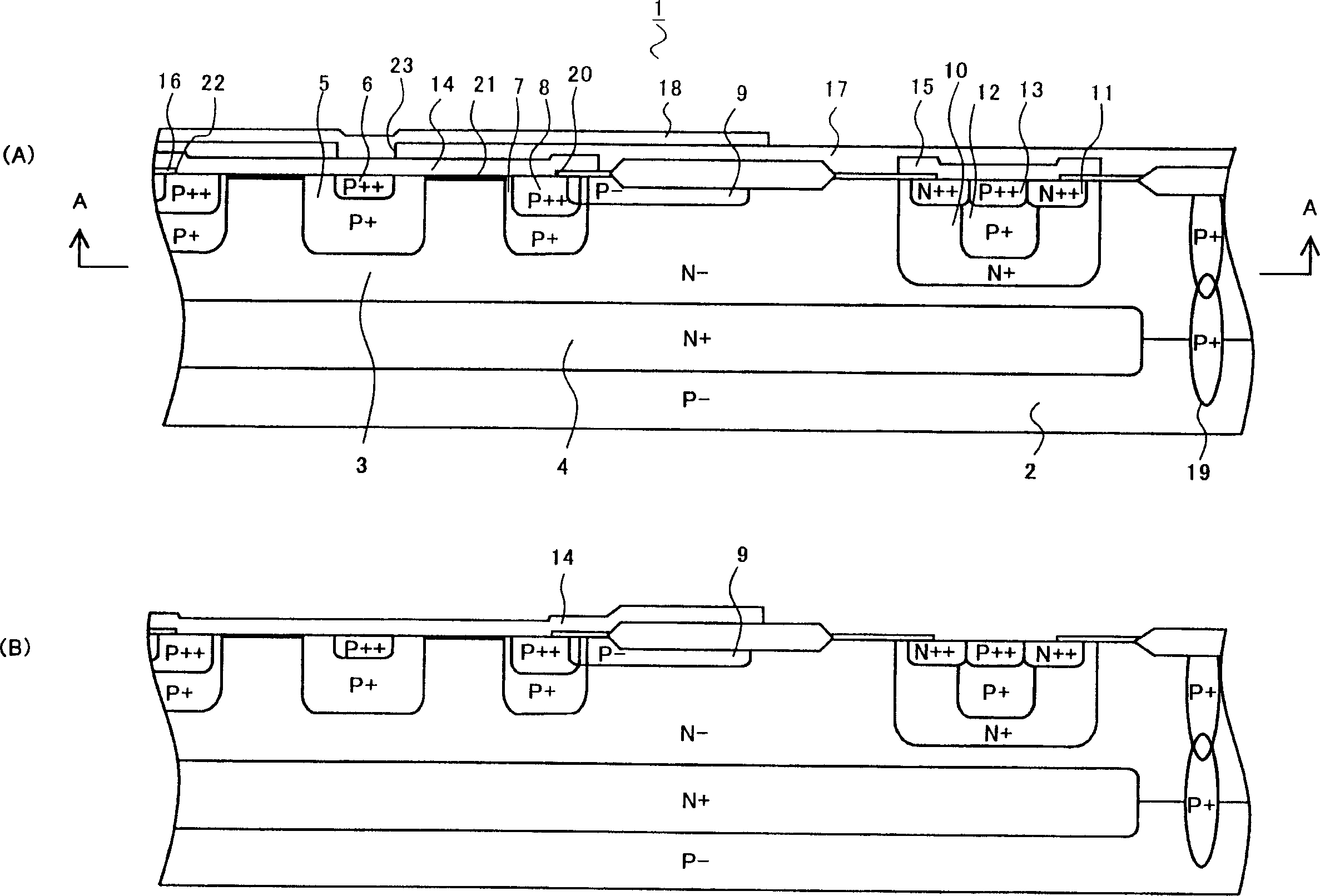
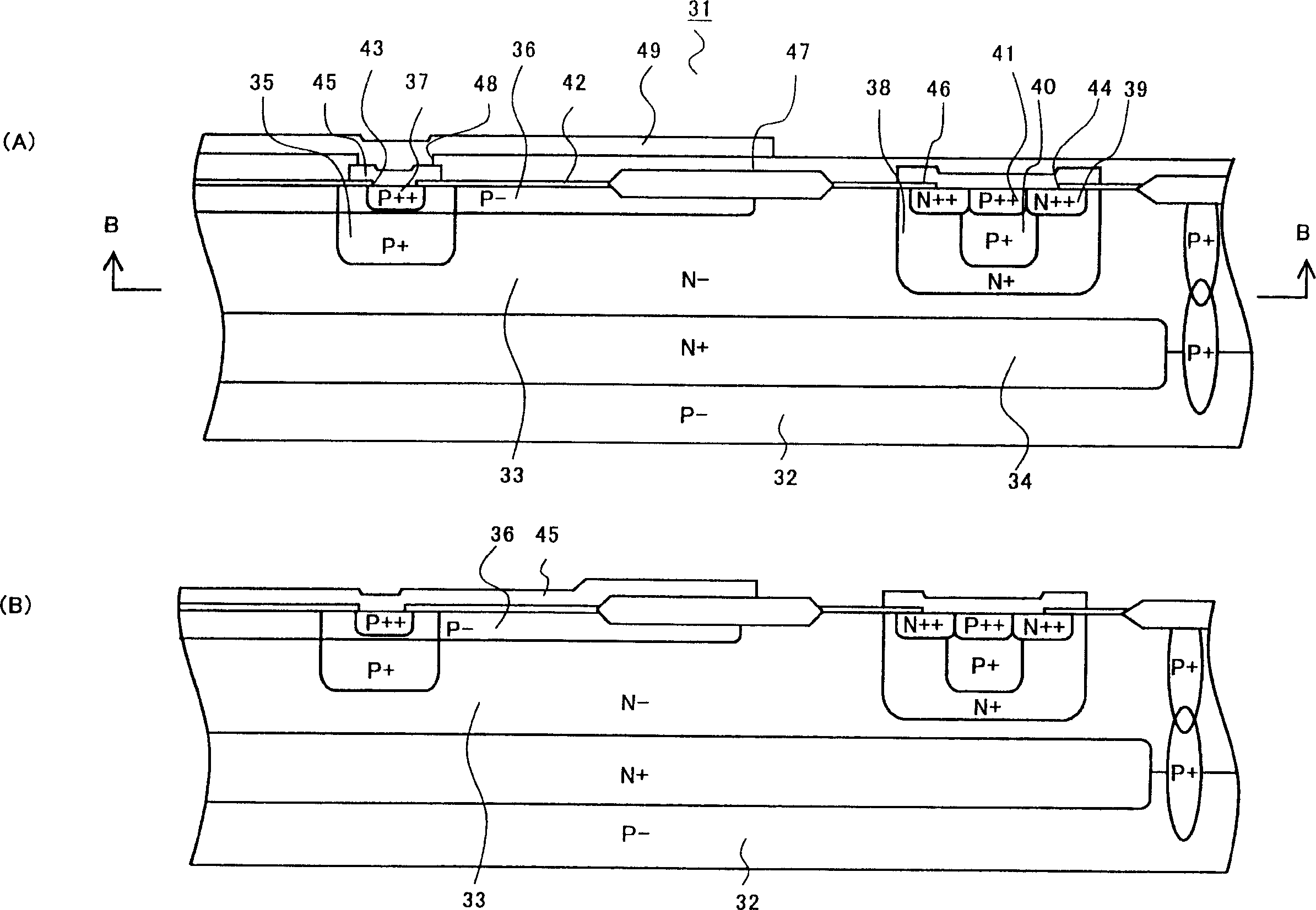
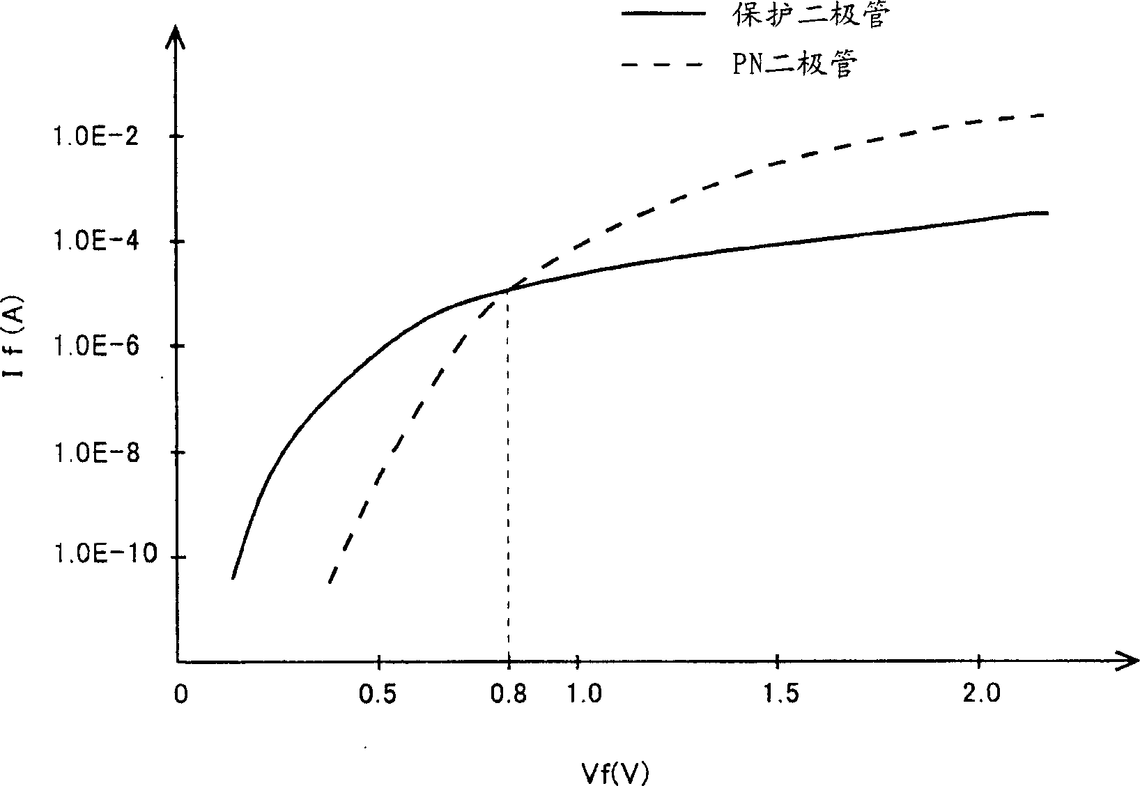
[0045] Below, refer to the attached Figure 1-7 , an embodiment of the semiconductor device of the present invention will be described in detail. figure 1 (A) and (B) are sectional views for explaining the protection diode of this embodiment. figure 2 (A) and (B) are sectional views for explaining the Zener diode of this embodiment. image 3 It is a graph explaining the forward voltage (Vf) of the protection diode and Zener diode of this embodiment. Figure 4 It is a figure explaining the circuit incorporating the protection diode of this embodiment. Figure 5 (A) is a diagram illustrating the potential distribution in a reverse bias state with respect to the protection diode of the present embodiment. Figure 5 (B) is a figure explaining the impact ionization generation region on the protection diode of this embodiment. Figure 6 This is a diagram illustrating potential distribution in a reverse bias state with respect to the protection diode of this embodiment. Figure...


PUM


Abstract

In a semiconductor device of the present invention, a protection diode for protecting a device is formed on an epitaxial layer formed on a substrate. A Schottky barrier metal layer is formed on a surface of the epitaxial layer and a P-type diffusion layer is formed at a lower portion of an end portion of the Schottky barrier metal layer. Then, a P-type diffusion layer is formed to be connected to a P-type diffusion layer and is extended to a cathode region. A metal layer to which an anode electrode is applied is formed above the P-type diffusion layer, thereby making it possible to obtain a field plate effect. This structure reduces a large change in a curvature of a depletion layer, thereby improving a withstand voltage characteristic of the protection diode.

Description

technical field [0001] The present invention relates to semiconductor devices for protecting circuit elements from overvoltage damage. Background technique [0002] In conventional semiconductor devices, an N-type epitaxial layer is formed on an N-type semiconductor substrate. A P-type diffusion layer is formed superimposed on the N-type diffusion layer formed on the epitaxial layer. Furthermore, an anode electrode is formed on the P-type diffusion layer, and a cathode electrode is formed on the back surface of the substrate, and a Zener diode is formed by utilizing the PN junction of the two diffusion layers. A P-type guard region is formed around the P-type diffusion layer, and another guard region is formed outside it. In addition, a Schottky barrier metal layer is formed in contact with the epitaxial layer surrounded by the two guard regions. A Schottky barrier diode is composed of a silicide and an epitaxial layer of a metal layer for a Schottky barrier. In a conven...

Claims


Application Information

Patent Timeline
IPC IPC(8): H01L29/861
Inventor 菊地修一大川重明中谷清史高桥利幸
Owner SANYO ELECTRIC CO LTD
Why Eureka
Try Eureka