Method for mfg. metal silicide

A technology of metal silicide and manufacturing method, which is applied in semiconductor/solid-state device manufacturing, electrical components, circuits, etc., and can solve problems such as spikes and lateral diffusion, interface leakage current, and nickel inapplicability

Inactive Publication Date: 2006-11-15
UNITED MICROELECTRONICS CORP
View PDF0 Cites 5 Cited by
  • Summary
  • Abstract
  • Description
  • Claims
  • Application Information

AI Technical Summary

Problems solved by technology

However, the above method is not suitable for nickel
Because during the second tempering, NiSi will react into NiSi because the temperature is too high 2 , resulting in spikes and lateral dif

Method used


Image

  • Method for mfg. metal silicide
  • Method for mfg. metal silicide
  • Method for mfg. metal silicide

Examples


Embodiment Construction

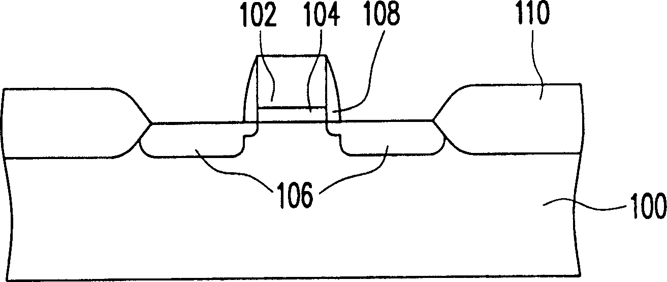
[0037] Figure 1A to Figure 1E It is a flow sectional view of a metal silicide manufacturing method according to a preferred embodiment of the present invention. First, please refer to Figure 1A , a silicon substrate 100 is provided, and an active area (active area) is defined on the substrate 100 by an isolation structure 110 . The isolation structure 110 is, for example, a field oxide layer formed by a local area thermal oxidation method or a shallow trench isolation structure formed by a shallow trench isolation method. A metal-oxide-semiconductor transistor is formed in the active region, and the metal-oxide-semiconductor transistor includes a drain / source 106, a gate 102, and a gate oxide layer 104 below the gate 102, and is formed on the sidewall of the gate 102. There is a spacer wall 108 .

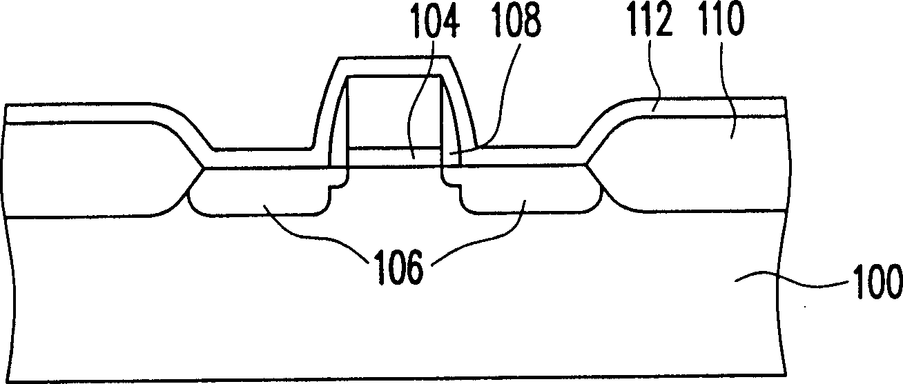
[0038] Next, please refer to Figure 1B On the substrate 100, a metal layer 112 is deposited, and the material of the metal layer 112 includes heat-resistant metals, such as ti...


PUM


Abstract

This invention relates to one metal silicide manufacturing method. This invention is used to metal silicide technique. It is used to deposition anti heat metal layer and the layer is first back fired and the unreacted metal is eliminated. Species injection technique is done to inject the species into the metal silicide to destroy lattice structure in the metal silicide, that is done to avoid spiking and lateral diffusion brought by high temperature of the metal silicide when the second back fire, and the junction leakage problem generated is also avoided.

Description

technical field [0001] The present invention relates to a method for forming a metal silicide, in particular to a method for manufacturing a self-aligned-silicide (salicide). Background technique [0002] In semiconductor technology, a metal-oxide-semiconductor (MOS) transistor is composed of three electrodes including a gate, a source and a drain. The early MOS was composed of three layers of materials such as a metal layer, a silicon dioxide layer and a silicon substrate. However, since most metals have poor adhesion to silicon dioxide, polysilicon, which has better adhesion to silicon dioxide, has been proposed to replace the metal layer. However, the use of polysilicon has a problem that the resistance value is too high. Even if polysilicon is doped, its resistance is still too high to be suitable for replacing the metal layer of MOS. Later, a solution was proposed, which is to add a layer of metal silicide on the surface of the polysilicon with a thickness equal to t...

Claims


Application Information

Patent Timeline
IPC IPC(8): H01L21/3205H01L21/321H01L21/336H01L21/8234
Inventor 谢朝景江怡颖黄建中曹博昭徐新惠林建廷戎乐天
Owner UNITED MICROELECTRONICS CORP
Why Eureka
Try Eureka