Check patentability & draft patents in minutes with Patsnap Eureka AI!

NOR flash memory and manufacture method thereof

A manufacturing method and memory technology, which are applied in semiconductor/solid-state device manufacturing, electric solid-state devices, semiconductor devices, etc., can solve the problem that the area of ​​NOR-type flash memory cannot be further reduced, and achieve the effect of reducing the array area.

Inactive Publication Date: 2010-07-21
MACRONIX INT CO LTD
View PDF3 Cites 0 Cited by
  • Summary
  • Abstract
  • Description
  • Claims
  • Application Information

AI Technical Summary

Problems solved by technology

[0005] However, because the above-mentioned structure has a lot of contact windows, it is necessary to reserve a lot of contact window areas connected to the drain region when designing the array structure, resulting in that the area of ​​the NOR flash memory cannot be further reduced, and compared with the current miniaturization of semiconductors. contrary to the trend of development

Method used


Image

  • NOR flash memory and manufacture method thereof
  • NOR flash memory and manufacture method thereof
  • NOR flash memory and manufacture method thereof

Examples


no. 1 example

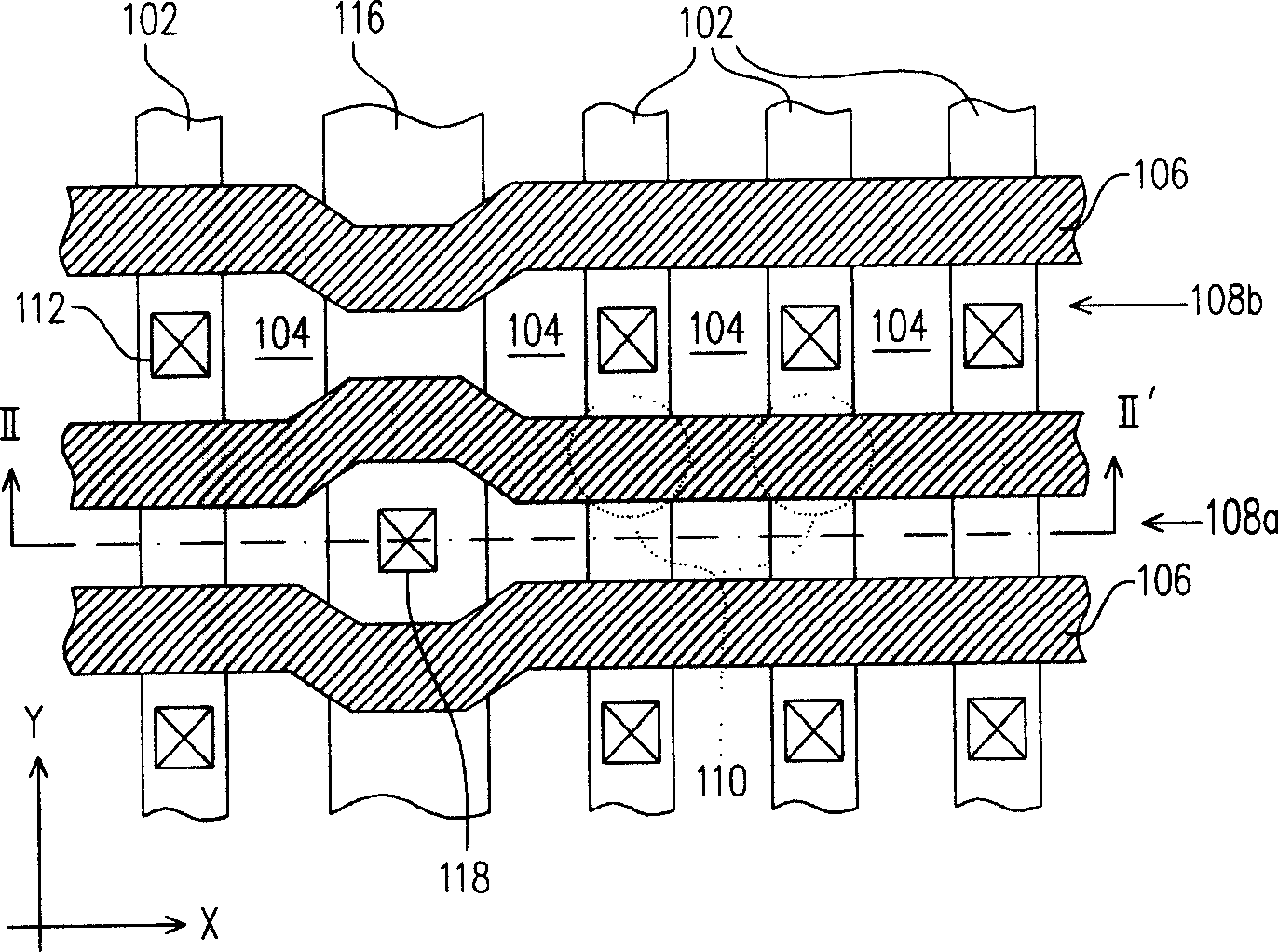
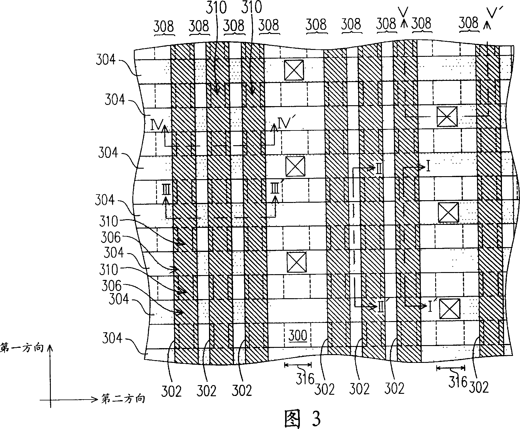
[0050] FIG. 3 is a top view of a NOR flash memory body according to a first embodiment of the present invention. Figure 4-I , Figure 4-II , Figure 4-III and Figure 4-IV Then it is respectively the sectional view of I-I' line segment, II-II' line segment, III-III' line segment and IV-IV' line segment in Fig. 3 .

[0051] Please refer to Figure 3 together with Figure 4-I , Figure 4-II , Figure 4-III and Figure 4-IV As shown, the NOR flash memory body of this embodiment is basically composed of a substrate 300, several control gates 302, several doped regions 304, isolation layers 306, several isolation structures 308, and multiple floating gates. 310 . The tunneling dielectric layer 312 and the inter-gate dielectric layer 314 are formed. Wherein, the control gate 302 is arranged on the substrate 300 in a first direction, and the doped region 304 is arranged in the substrate 300 in a second direction, and in the NOR flash memory body of this embodiment, the doped reg...

no. 2 example

[0057] The manufacturing process of the NOR flash memory body of the present invention will be described in detail later, but it is only used as an example of the application of the present invention, rather than limiting the present invention to the following methods. In addition, if the "main component symbol" used below is the same as that of each previous figure, it represents the same or a similar component.

[0058] Figures 6A-I to Figure 6D-I It is a sectional view of the manufacturing process of the I-I' line segment of Fig. 3. Figure 6A-II to Figure 6E-II It is a sectional view of the manufacturing process of the II-II' line segment in Fig. 3 . Figure 6A-III to Figure 6E-III It is a sectional view of the manufacturing process of the III-III' line segment in Fig. 3 . Figures 6A-IV to Figure 6E-IV It is a sectional view of the manufacturing process of the IV-IV' line segment of Fig. 3 .

[0059] Please also refer to FIGS. 6A-I to 6A-IV. In a substrate 300, sev...


PUM


Abstract

This invention relates to NOR type flash memory bank, it is made up by basement, control gate, doping area, separator layer, separator structure, floating gate, tunneling dielectric layer and intergate dielectric layer. The control gate is arrayed on the basement as first orientation; the doping area is arrayed on the basement as the second orientation. The separating layer is set between the control gate and the doping area, but the separating structure is set in the basement out of the doping area and the control gate. The floating gate is set between the basement among the separating layerand the control pole, the tunneling dielectric layer is set between basement and floating pole, intergate dielectric layer is set between control and floating poles.

Description

technical field [0001] The present invention relates to a flash memory body, and in particular to a NOR-type flash memory (NOR-type flash memory) and a manufacturing method thereof. Background technique [0002] Flash memory components have the advantages of being able to store, read, and erase data multiple times, and the stored data will not disappear after power failure, so it has become widely used in personal computers and electronic devices. A non-volatile memory element used. [0003] see figure 1 Shown is a top view of a known NOR flash memory body, and figure 2 yes figure 1 Sectional view of line II-II'. [0004] Please also see figure 1 and figure 2 As shown, there are diffusion regions 102 and isolation structures 104 arranged alternately in the y direction in the substrate 100 , and there are control gates 106 arranged at intervals in the x direction on the substrate 100 . The floating gate (not shown) and the tunneling dielectric layer (not shown) in th...

Claims


Application Information

Patent Timeline
Patent Type & Authority Patents(China)
IPC IPC(8): H01L21/8247H01L21/8234H01L27/105
Inventor 林新富吴俊沛
Owner MACRONIX INT CO LTD
Features
  • R&D
  • Intellectual Property
  • Life Sciences
  • Materials
  • Tech Scout
  • Unparalleled Data Quality
  • Higher Quality Content
  • 60% Fewer Hallucinations
Learn More