

UV curing apparatus for group substrate
An irradiation device and ultraviolet light technology, which is applied in identification devices, optics, nonlinear optics, etc., can solve the problems of low average illuminance value of long ultraviolet light tubes, increased difficulty of illuminance monitoring in manufacturing process, and increased cost.
- Summary
- Abstract
- Description
- Claims
- Application Information
AI Technical Summary
Problems solved by technology
Method used
Image

Examples
no. 1 example
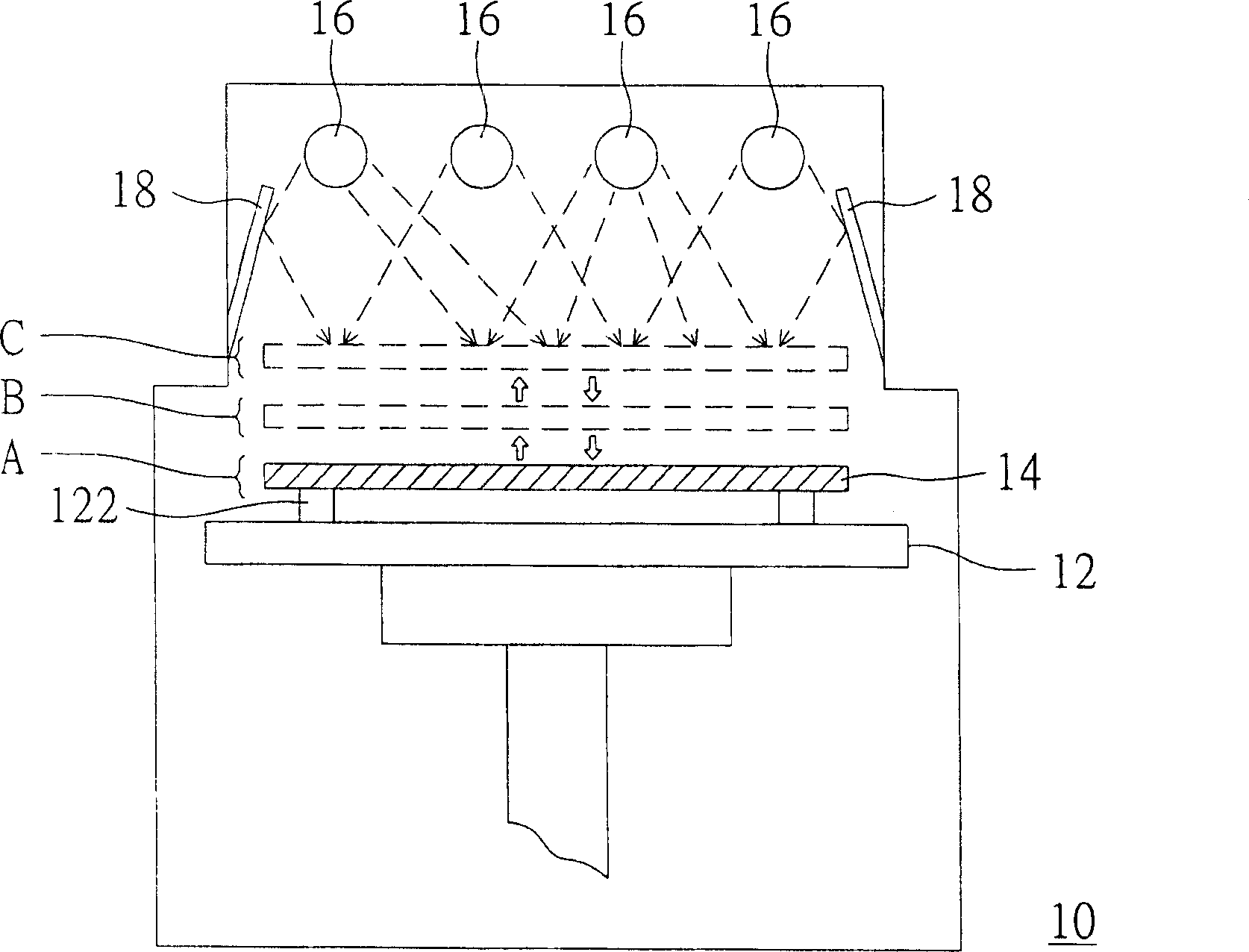
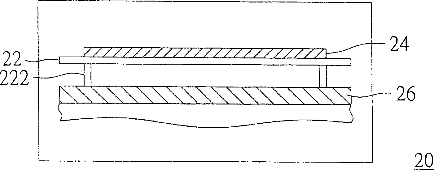
[0041] Please refer to figure 2 , which is a simple schematic diagram of an ultraviolet light irradiation device (UV) according to the first embodiment of the present invention. The ultraviolet light irradiation device 20 of the first embodiment uses a carrying portion 22 to carry a pair of motherboards 24 to be irradiated, wherein the pair of motherboards 24 may include one or more panels. In the irradiation device 20 , the optical part for illuminating the pair of motherboards 24 includes a backlight module 26 , so that the ultraviolet light can be uniformly irradiated to the motherboard 24 . In addition, a lifting device 222 may be further provided on the carrying portion 22 so that the carrying portion 22 and the backlight module 26 are separated by an appropriate distance.
[0042] In the first embodiment, the backlight module 26 is disposed under the motherboard 24 to irradiate ultraviolet light from bottom to top. image 3 It is a schematic diagram of the first backl...
no. 2 example
[0057] Please refer to Figure 5 , which is a simple schematic diagram of an ultraviolet light irradiation device (UV) according to the second embodiment of the present invention. The difference between the second embodiment and the first embodiment is that the ultraviolet light irradiation device 20 of the first embodiment has a group of backlight modules 26 arranged under the motherboard 24, while the ultraviolet light irradiation device 40 of the second embodiment has two A group of backlight modules are respectively arranged on the upper and lower sides of the motherboard 44 to simultaneously irradiate both sides with ultraviolet light. Likewise, motherboard 24 may include one or more panels.
[0058] Figure 5 Among them, the first backlight module 45 is located below the motherboard 44, so that the light of ultraviolet light irradiates the motherboard 44 from bottom to top through the light guide plate, and the second backlight module 46 is located above the motherboar...
no. 3 example
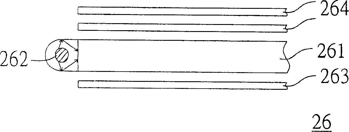
[0063] Figure 6A It is a combination of a light guide plate and a long lamp tube according to the third embodiment of the present invention. Figure 6B It is a combination of a light guide plate and a point light source according to the third embodiment of the present invention. In the third embodiment, the combination of light guide plates is composed of multiple light guide plates in an n×m matrix, where n and m are positive integers greater than 1, and n and m can be equal or different, and there is no special limitation . As for the light source, either a long lamp tube or a point light source can be used, and its position corresponds to the position of the light guide plates so that the light can reach the light guide plates.
[0064] Figure 6A The central system uses a plurality of elongated lamp tubes 562 as light sources, and their installation positions are, for example, corresponding to the junctions of the light guide plates 561 . The elongated lamp tubes 562 ...
PUM
 Abstract
Description
Claims
Application Information