Schottky barrier integrated circuit

A Schottky potential, integrated circuit technology, used in circuits, electrical components, transistors, etc.

Inactive Publication Date: 2006-11-29
SPINNAKER SEMICON
View PDF6 Cites 3 Cited by
  • Summary
  • Abstract
  • Description
  • Claims
  • Application Information

AI Technical Summary

Problems solved by technology

[0008] Despite these attempts, there is no known reference teaching that a fabricated integrated circuit with at least one Schottky barrier MOSFET device (Schottky barrier integrated circuit) has been tested and reported

Method used


Image

  • Schottky barrier integrated circuit
  • Schottky barrier integrated circuit
  • Schottky barrier integrated circuit

Examples


Embodiment Construction

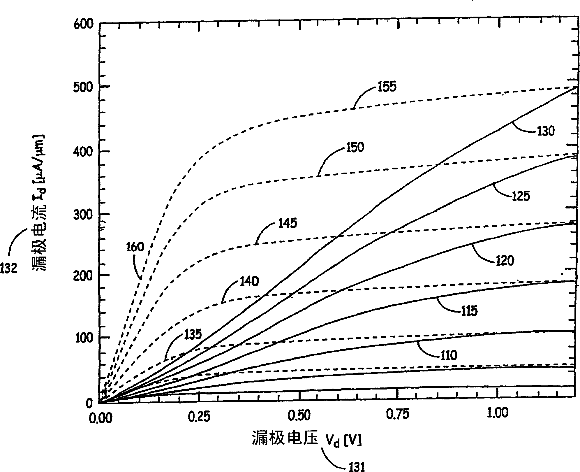
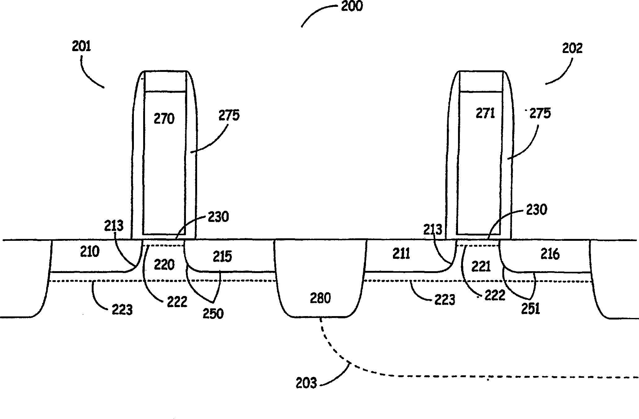
[0023]Generally, the present invention provides integrated circuits. The integrated circuit consists of at least one NMOS device or at least one PMOS device; wherein the at least one NMOS device or at least one PMOS device is a Schottky barrier MOS device with bulk charge transport. In one embodiment, the Schottky barrier BMOS and Schottky barrier PMOS devices each consist of a semiconductor substrate and a gate electrode on the semiconductor substrate. Source and drain electrodes on the semiconductor substrate define a channel region having a channel length and having mobile charge carriers, wherein at least one of the source and drain electrodes forms a Schottky connection with the substrate base or Schottky-like contacts.

[0024] As a unique advantage, the inventors have discovered that metal source and drain electrodes can greatly reduce parasitic series resistance (~10 Ω-μm) and contact resistance (less than 10 -8 Ω-cm 2 ). The built-in Schottky barrier at the Schott...


PUM


Abstract

A Schottky barrier integrated circuit is disclosed, the circuit having at least one PMOS device or at least one NMOS device, at least one of the PMOS device or NMOS device having metal source-drain contacts forming Schottky barrier or Schottky-like contacts to the semiconductor substrate. The device provides a new distribution of mobile charge carriers in the bulk region of the semiconductor substrate, which improves device and circuit performance by lowering gate capacitance, improving effective carrier mobility, mu reducing noise, reducing gate insulator leakage, reducing hot carrier effect and improving reliability.

Description

(1) Technical field [0001] The present invention generally relates to the field of semiconductor integrated circuits (ICs). More specifically, the present invention relates to a metal oxide semiconductor field effect transistor (MOSFET) having a Schottky barrier and including at least one Schottky barrier P-type MOSFET (PMOS) or N-type MOSFET (NMOS) and / or a Schottky barrier Turki-barrier complementary MOSFET (CMOS) ICs. (2) Background technology [0002] One type of transistor known in the art is the Schottky barrier metal oxide semiconductor field effect transistor (Schottky barrier MOSFET or SB-MOS). The source and drain electrodes of the SB-MOS device are made of metal. A Schottky barrier contact is formed at the interface between the metal and semiconductor substrate. Another transistor known in the prior art is the conventional metal oxide semiconductor field effect transistor (conventional MOSFET). In contrast to SB-MOS devices, the source and drain electrodes of ...

Claims


Application Information

Patent Timeline
Patent Type & Authority Applications(China)
IPC IPC(8): H01L27/095H01L29/78H01L21/336
Inventor J·P·斯奈德J·M·拉森
Owner SPINNAKER SEMICON
Why Eureka
Try Eureka