Liquid crystal device and electronic apparatus
A technology of liquid crystal device and liquid crystal layer, which is applied in the direction of TV, electrical components, color TV, etc., can solve the problems such as not being able to obtain good display
- Summary
- Abstract
- Description
- Claims
- Application Information
AI Technical Summary
Problems solved by technology
Method used
Image

Examples
no. 1 Embodiment approach
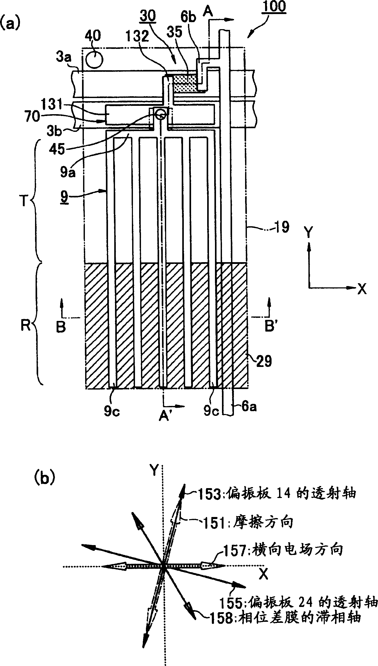
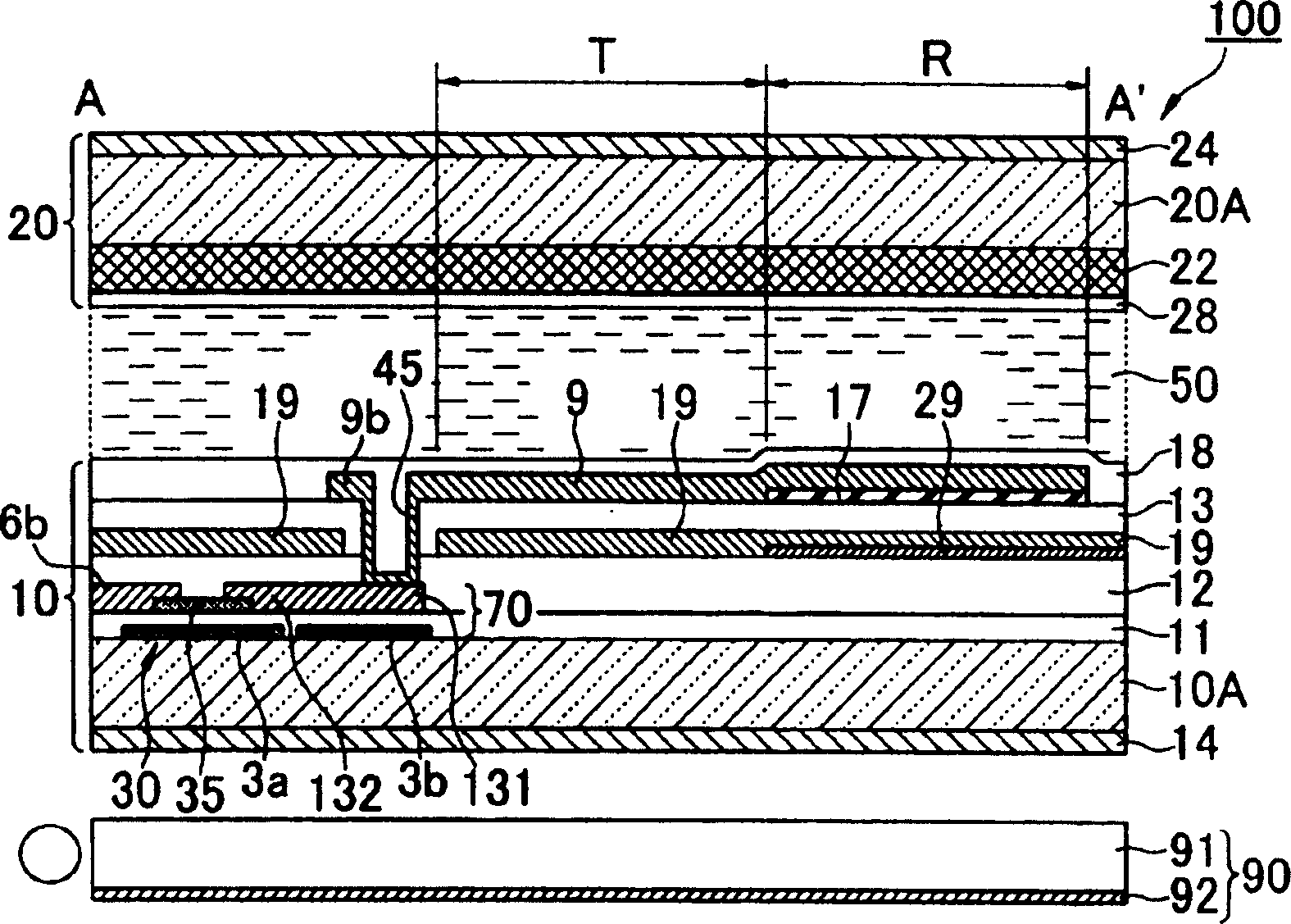
[0031] Hereinafter, a liquid crystal device according to a first embodiment of the present invention will be described with reference to the drawings. The liquid crystal device of this embodiment is one of the lateral electric field methods in which images are displayed by applying an electric field in the direction of the substrate surface (lateral electric field) to the liquid crystal to control alignment. ) mode of the liquid crystal device.
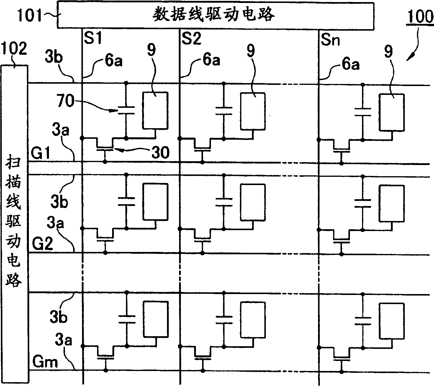
[0032] In addition, the liquid crystal device of this embodiment is a color liquid crystal device provided with a color filter on a substrate, and one pixel is constituted by three sub-pixels that output light of each color of R (red), G (green), and B (blue). . Therefore, a display area constituting the smallest unit constituting a display is referred to as a "sub-pixel area", and a display area composed of a set of (R, G, B) sub-pixels is referred to as a "pixel area".
[0033] figure 1 , is a circuit configuration diagram of a p...
no. 2 Embodiment approach
[0069] Second, refer to Figure 5 A second embodiment of the present invention will be described. Figure 5 (a) is a partial cross-sectional configuration diagram of a liquid crystal device 201 according to the first configuration example of the present embodiment; Figure 5 (b) is a partial sectional configuration diagram of a liquid crystal device 202 according to a second configuration example of the same embodiment. The liquid crystal devices 201 and 202 of this embodiment both have the same basic configuration as the liquid crystal device 100 of the first embodiment, except that the second interlayer insulating film 13 provided between the pixel electrode 9 and the common electrode 19, It is formed to have different film thicknesses in the sub-pixel area. Thus, in Figure 5 in, right and from Figure 1 to Figure 4 Components that are the same as those of the liquid crystal device 100 shown in FIG.
[0070] First of all, yes Figure 5 The liquid crystal device 201 of...
no. 3 Embodiment approach
[0087] Second, refer to Image 6 A third embodiment of the present invention will be described. Image 6 , is a diagram showing a schematic planar configuration of the sub-pixel region of the liquid crystal device 300 of the present embodiment.
[0088] The liquid crystal device 300 of this embodiment adopts the Image 6 The pixel electrode 39 having the configuration shown in 2 is used instead of the pixel electrode 9 in the liquid crystal device 100 of the first embodiment, and the other configurations are the same as those of the liquid crystal device 100 . Thus, in Image 6 From and to Figure 1 to Figure 4 The same components are denoted by the same symbols, and their detailed descriptions are omitted.
[0089] exist Image 6 The pixel electrode 39 shown in , has a plurality of (ten in the figure) strip-shaped electrodes 39c, and each strip-shaped electrode 39c is electrically connected to each other and is electrically connected to the TFT. The pixel electrode 39 o...
PUM
| Property | Measurement | Unit |
|---|---|---|
| thickness | aaaaa | aaaaa |
| relative permittivity | aaaaa | aaaaa |
| relative permittivity | aaaaa | aaaaa |
Abstract
Description
Claims
Application Information