Method of manufacturing semiconductor device

a manufacturing method and semiconductor technology, applied in the direction of coatings, metallic material coating processes, chemical vapor deposition coatings, etc., can solve the problems of low etching rate, increased permittivity, leak resistance deterioration, etc., and achieve low etching rate, low etching rate, and high insulating property.

Active Publication Date: 2016-01-14
KOKUSA ELECTRIC CO LTD
View PDF3 Cites 3 Cited by
  • Summary
  • Abstract
  • Description
  • Claims
  • Application Information

AI Technical Summary

Benefits of technology

[0007]When carbon is added to insulating films, the etching resistance of the insulating films is improved, but permittivity is increased and leak resistance is deteriorated. That is, each of the insulating films has advantages and defects, but in the related art, there is no film having characteristics such as low permittivity, a low etching rate, and a high insulating property.
[0008]Accordingly, it is an aspect of the present invention to provide a method of manufacturing a semiconductor device, a method of processing a substrate and a substrate processing apparatus capable of forming an insulating film having low permittivity, a low etching rate, and a high insulating property.
[0012]According to the present invention, an insulating film having low permittivity, a low etching rate, and a high insulating property can be formed.

Problems solved by technology

When carbon is added to insulating films, the etching resistance of the insulating films is improved, but permittivity is increased and leak resistance is deteriorated.
That is, each of the insulating films has advantages and defects, but in the related art, there is no film having characteristics such as low permittivity, a low etching rate, and a high insulating property.

Method used


Image

  • Method of manufacturing semiconductor device
  • Method of manufacturing semiconductor device
  • Method of manufacturing semiconductor device

Examples


example

First Example

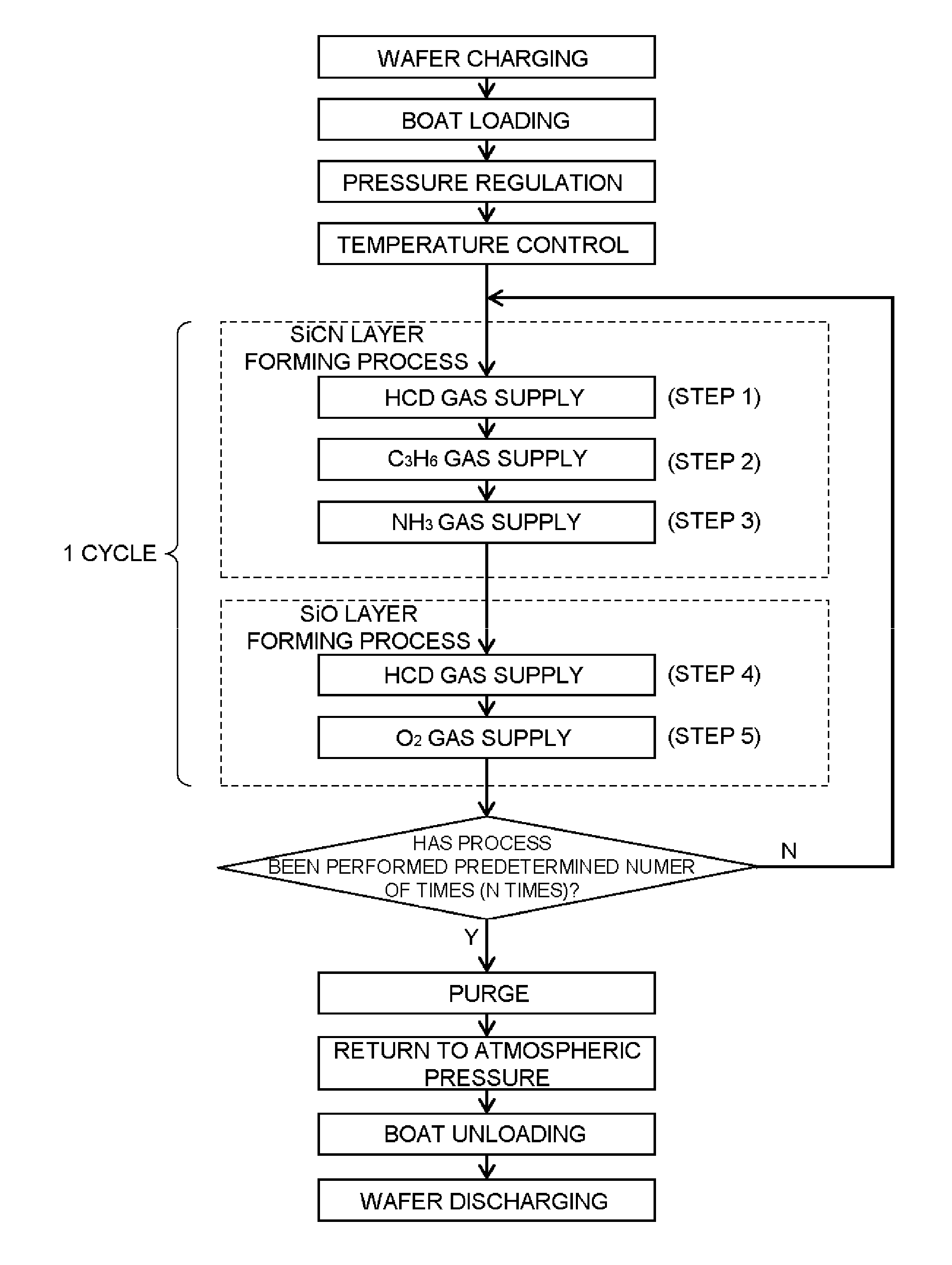
[0186]A SiOCN film was formed while controlling a composition ratio by the first sequence according to the embodiment, and a composition ratio of the SiOCN film and film thickness uniformity in a wafer surface were measured. HCD gas, which is a silicon-containing gas, C3H6 gas, which is a carbon-containing gas, NH3 gas, which is a nitrogen-containing gas, and O2 gas, which is an oxygen-containing gas, were used. Control of the composition ratio of the SiOCN film was performed by adjusting a pressure and gas supply time (irradiation time), which are parameters for controlling the composition ratio.

[0187]First, the pressure in the processing chamber in a second step of the first sequence and C3H6 gas supply time of the second step were adjusted, and the SiOCN film having a carbon concentration of about 8 atoms % was formed on a wafer. The processing conditions at this time were set as the following conditions.

[0188]

[0189](First Step)

[0190]Temperature in processing chamber...

second example

[0271]A SiOCN film was formed while controlling a composition ratio by the second sequence of the above-mentioned embodiment, and the composition ratio of the SiOCN film and film thickness uniformity in the wafer surface were measured. HCD gas, which is a silicon-containing gas, C3H6 gas, which is a carbon-containing gas, NH3 gas, which is a nitrogen-containing gas, and O2 gas, which is an oxygen-containing gas, were used. The processing conditions in each step were set to the same processing conditions as each step of the standard processing conditions of the first example. Control of the composition ratio of the SiOCN film was performed by adjusting each set number in the second sequence, i.e., a set number (x) of a SiCN layer forming process and a set number (y) of a SiO layer forming process.

[0272]As a result, when the set number (x) of the SiCN layer forming process in the second sequence was set to 2 and the set number (y) of the SiO layer forming process was set to 1 (x=2, y=...


PUM

PropertyMeasurementUnit
pressureaaaaaaaaaa
timeaaaaaaaaaa
temperatureaaaaaaaaaa

Abstract

An insulating film including characteristics such as low permittivity, a low etching rate and a high insulation property is formed. Supplying a gas containing an element, a carbon-containing gas and a nitrogen-containing gas to a heated substrate in a processing vessel to form a carbonitride layer including the element, and supplying the gas containing the element and an oxygen-containing gas to the heated substrate in the processing vessel to form an oxide layer including the element are alternately repeated to form on the substrate an oxycarbonitride film having the carbonitride layer and the oxide layer alternately stacked therein.

Description

CROSS-REFERENCE TO RELATED PATENT APPLICATION[0001]This U.S. non-provisional patent application is a continuation of U.S. patent application Ser. No. 13 / 345,885 filed on Jan. 9, 2012 and claims priority under 35 U.S.C. §119 of Japanese Patent Applications No. 2011-005638 filed on Jan. 14, 2011 and No. 2011-268002 filed on Dec. 7, 2011, in the Japanese Patent Office, the entire contents of which are hereby incorporated by reference.BACKGROUND OF THE INVENTION[0002]1. Field of the Invention[0003]The present invention relates to a method of manufacturing a semiconductor device including a process of forming a thin film on a substrate, a method of processing a substrate and a substrate processing apparatus.[0004]2. Description of the Related Art[0005]A process of manufacturing a semiconductor device includes a process of forming a silicon insulating film such as a silicon oxide film (a SiO2 film, hereinafter referred to as a SiO film) or a silicon nitride film (a Si3N4 film, hereinafter...

Claims


Application Information

Patent Timeline
Patent Type & Authority Applications(United States)
IPC IPC(8): H01L21/02
CPCH01L21/0228H01L21/02112H01L21/02167C23C16/30C23C16/36C23C16/40C23C16/401C23C16/45523C23C16/45529C23C16/45531C23C16/45546H01L21/02126H01L21/0217H01L21/02211
Inventor HIROSE, YOSHIROTAKASAWA, YUSHINKAMAKURA, TSUKASANAKAMURA, YOSHINOBUSASAJIMA, RYOTA
Owner KOKUSA ELECTRIC CO LTD
Why Eureka
Try Eureka