

Antenna pattern and electromagnetic wave energy processing device having the same
An antenna pattern and energy processing technology, applied in antennas, antenna parts, circuits, etc., can solve problems such as electromagnetic wave effects, achieve clear and stable images, improve performance, and simplify pattern images.
- Summary
- Abstract
- Description
- Claims
- Application Information
AI Technical Summary
Problems solved by technology
Method used
Image

Examples
Embodiment 1
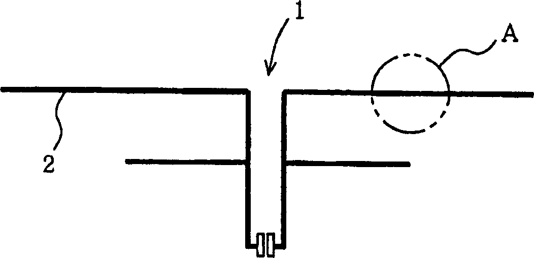
[0068] figure 1 It is a figure which shows the antenna pattern of Example 1 of this invention.
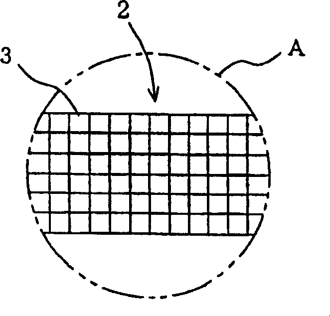
[0069] figure 2 yes figure 1 The enlarged reference figure of part A in , shows an example of the case where the collection line includes grid-shaped micropicture unit lines.
[0070] In the figure, 1 is an antenna pattern, 2 is a wire, and 3 is a mesh-like micropicture unit line.
[0071] The wire width of the antenna pattern in embodiment 1 is made as 2mm, and the length of the long wire portion is made as 39cm, and the length of the short wire portion is made as 25cm, and the interval between the two lines is made as 3cm, and the above-mentioned wire is made into a collection line of a grid pattern, The line width was set to 20 μm, the line spacing was set to 100 μm, and printing was performed by offset printing using a synthetic ink mixed with Pd powder having an average particle diameter of 1 μm. Cu plating with a thickness of approximately 1 μm was performed on the print...
Embodiment 2
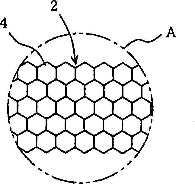
[0076] image 3 It is an enlarged reference diagram of part A in Embodiment 2 of the present invention, and shows an example of a case where the assembly line includes continuous polygonal miniature image unit lines.
[0077] In the figure, 4 is a continuous polygonal micropicture unit line.
[0078] The antenna pattern in embodiment 2 is the same as embodiment 1, and the wire width is 2mm, and the length of the long line is 39cm, and the length of the short line is 25cm, and the interval between the two lines is 3cm, and the above-mentioned wire is made into a collection of grid-like mesh patterns Lines were printed by offset printing with a synthetic ink mixed with Pd powder having an average particle diameter of 1 μm, with the line width set at 20 μm and the distance across sides of the continuous polygonal shape set at 100 μm. Cu plating with a thickness of approximately 1 μm was performed on the printed surface by an electroless method.
[0079] For comparison, as an an...
Embodiment 3
[0083] Figure 4 It is an enlarged reference diagram of part A in Embodiment 3 of the present invention, showing an example of a case where the assembly lines are parallel assembly lines.
[0084] In the figure, 5 is a parallel collection line of straight lines.
[0085] The antenna pattern in embodiment 3 is the same as that in embodiment 1, the wire width is 2mm, the length of the long line is 39cm, the length of the short line is 25cm, and the interval between the two lines is 3cm. The above-mentioned wires are made into parallel assembly lines. The line width was set to 20 μm, the line spacing was set to 100 μm, and printing was performed by offset printing using a synthetic ink mixed with Pd powder having an average particle diameter of 1 μm. Cu plating with a thickness of approximately 1 μm was performed on the printed surface by an electroless method.
[0086] For comparison, as an antenna pattern of the same image, an antenna pattern obtained by photolithographically...
PUM
| Property | Measurement | Unit |
|---|---|---|
| Line width | aaaaa | aaaaa |
| Line width | aaaaa | aaaaa |
| Line width | aaaaa | aaaaa |
Abstract
Description
Claims
Application Information