

Chuck workbench moving arrangement
A technology of chuck table and moving mechanism, which is applied in the direction of metal processing machinery parts, manufacturing tools, conveyor objects, etc., and can solve problems that may not be able to meet the high-precision movement of chuck table
- Summary
- Abstract
- Description
- Claims
- Application Information
AI Technical Summary
Problems solved by technology
Method used
Image

Examples
Embodiment Construction
[0020] Next, the preferred embodiment of the chuck table moving mechanism constructed according to the present invention will be described in more detail with reference to the accompanying drawings.
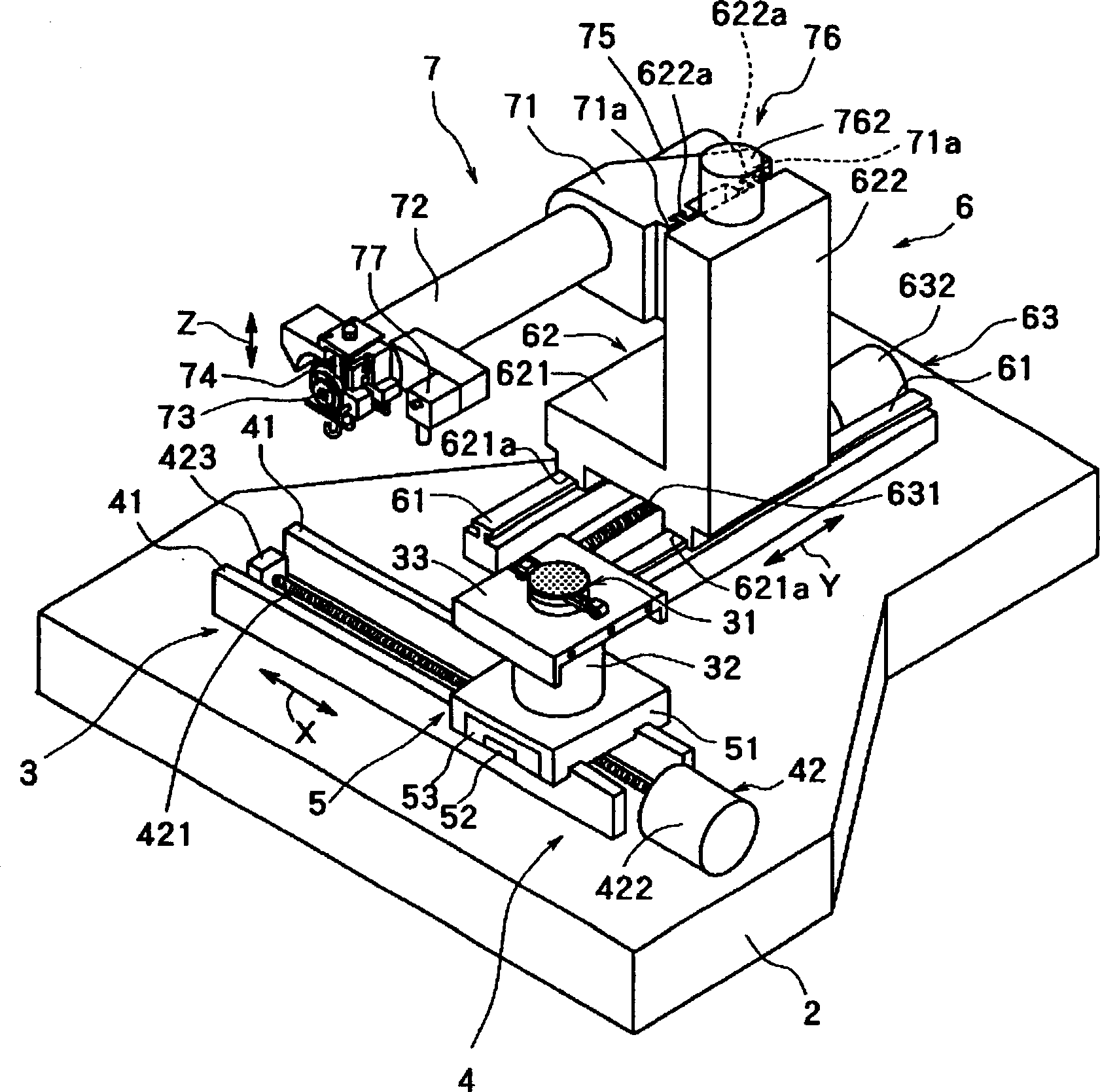
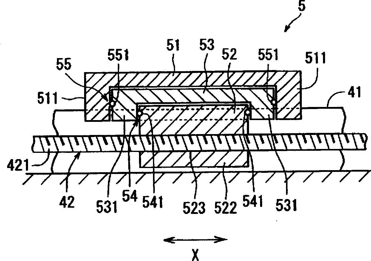
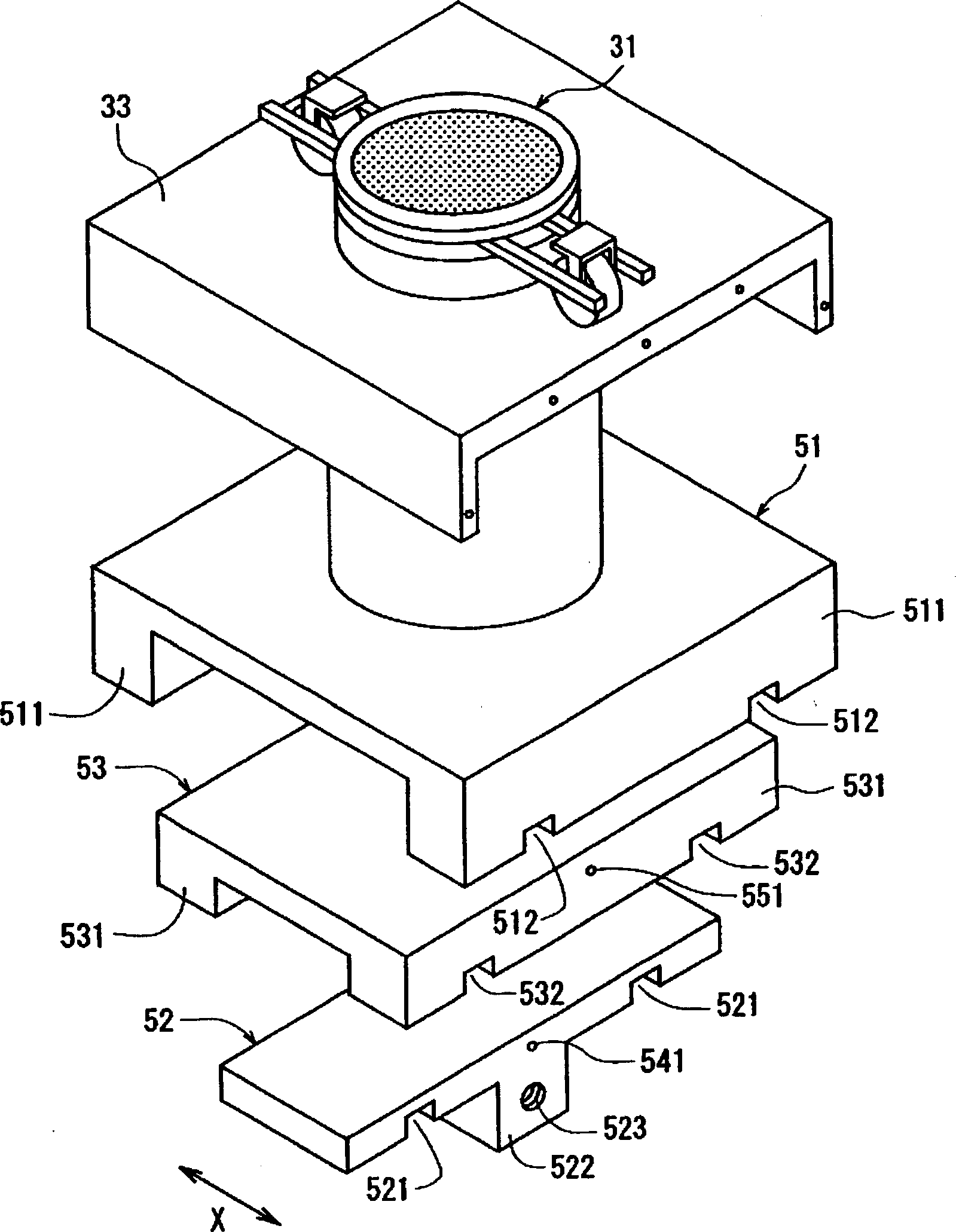
[0021] figure 1 It is a perspective view showing main parts of a cutting device equipped with a chuck table moving mechanism according to the present invention.
[0022] figure 1 The cutting device shown is equipped with: a stationary base 2; a chuck table mechanism 3 which is movably arranged on the stationary base 2 in the machining feed direction indicated by the arrow X to support the workpiece; In the indexing feed direction represented by arrow Y (the direction perpendicular to the processing feed direction represented by arrow X), the spindle supporting mechanism 6 that is movably arranged on the stationary base 2; A spindle assembly 7 serving as a cutting mechanism is movably arranged on the spindle support mechanism 6 in the tool depth feeding direction.
[0023] The ...
PUM
 Abstract
Description
Claims
Application Information