Production process tape for film-shaped wiring board
A technology for wiring substrates and production processes, which is applied in the field of tapes for production processes, can solve problems such as lower yields and increased product costs, and achieve the effects of avoiding cost increases and improving yields
- Summary
- Abstract
- Description
- Claims
- Application Information
AI Technical Summary
Problems solved by technology
Method used
Image

Examples
Embodiment
[0040] The present invention will be described in further detail below through examples and comparative examples, but the present invention is not limited to these examples. Raw materials used in Examples and Comparative Examples are as follows.
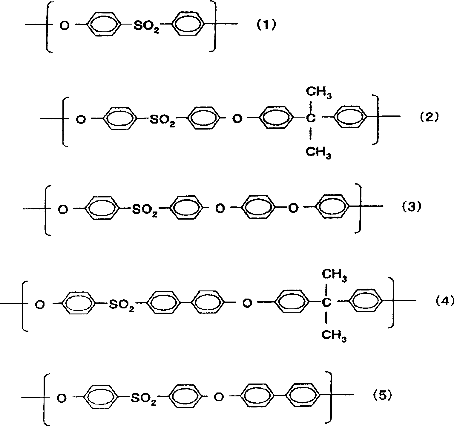
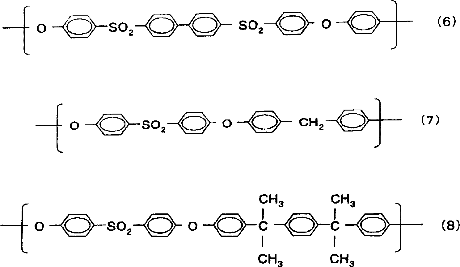
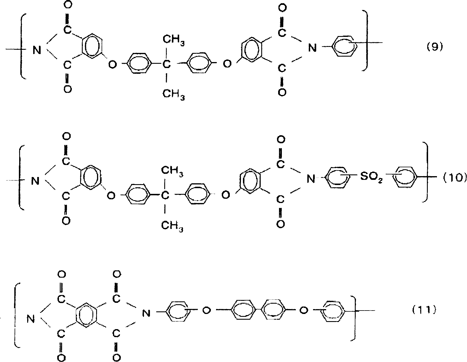
[0041] *1. Polysulfone resin
[0042] Udel P-1700NT (trade name) manufactured by Solvay Advanced Polymers
[0043] *2. Thermoplastic polyimide resin
[0044] ULTEM CRS5001-1000 made by GE
[0045] *3. Polyether aromatic ketone resin
[0046] PEEK450G (trade name) manufactured by VICTREX
[0047] *4. Glass fiber (fibrous)
[0048] RES-TP29 made by Asahi Glass Aspect ratio: 100 or more
[0049] *5. Alumina particles (granular)
[0050] AO-502 made by Admatechs Aspect ratio: 1
[0051] *6. Plate talc (plate shape)
[0052] Japan Talc MS-1 aspect ratio: 17, average particle size: 13μm
[0053] *7. Plate talc (plate shape)
[0054] Japan Talc L-1 aspect ratio: 25, average particle size: 5μm
[0055] According to the blending r...
PUM
| Property | Measurement | Unit |
|---|---|---|
| particle size | aaaaa | aaaaa |
| particle size | aaaaa | aaaaa |
Abstract
Description
Claims
Application Information
 - R&D Engineer
- R&D Manager
- IP Professional
- Industry Leading Data Capabilities
- Powerful AI technology
- Patent DNA Extraction
Browse by: Latest US Patents, China's latest patents, Technical Efficacy Thesaurus, Application Domain, Technology Topic.
© 2024 PatSnap. All rights reserved.Legal|Privacy policy|Modern Slavery Act Transparency Statement|Sitemap