Substrate topography compensation at mask design: 3D OPC topography anchored

a topography compensation and mask technology, applied in the field of semiconductor device manufacturing, can solve the problems of affecting the performance of the semiconductor device, the software is not effective for wafer topography correction or other process-induced critical dimension variation, and the quality of the semiconductor device is affected, so as to improve process precision, increase product yield rate, and improve the effect of quality

Inactive Publication Date: 2005-05-17
BELL SEMICON LLC
View PDF16 Cites 67 Cited by
  • Summary
  • Abstract
  • Description
  • Claims
  • Application Information

AI Technical Summary

Benefits of technology

[0006]Among the several objects of the present invention may be noted streamlining the semiconductor manufacturing processes, increasing product yield rates, solving the need for greater precision, improving process precision by means c...

Problems solved by technology

Processing deviations adversely affect the performance of a semiconductor device.
However, this software is not effective for wafer topography correction or other process-induced critical dimension (CD) variations.
Additional problems that cause optical proximity effects on the sur...

Method used


Image

  • Substrate topography compensation at mask design: 3D OPC topography anchored
  • Substrate topography compensation at mask design: 3D OPC topography anchored
  • Substrate topography compensation at mask design: 3D OPC topography anchored

Examples


Embodiment Construction

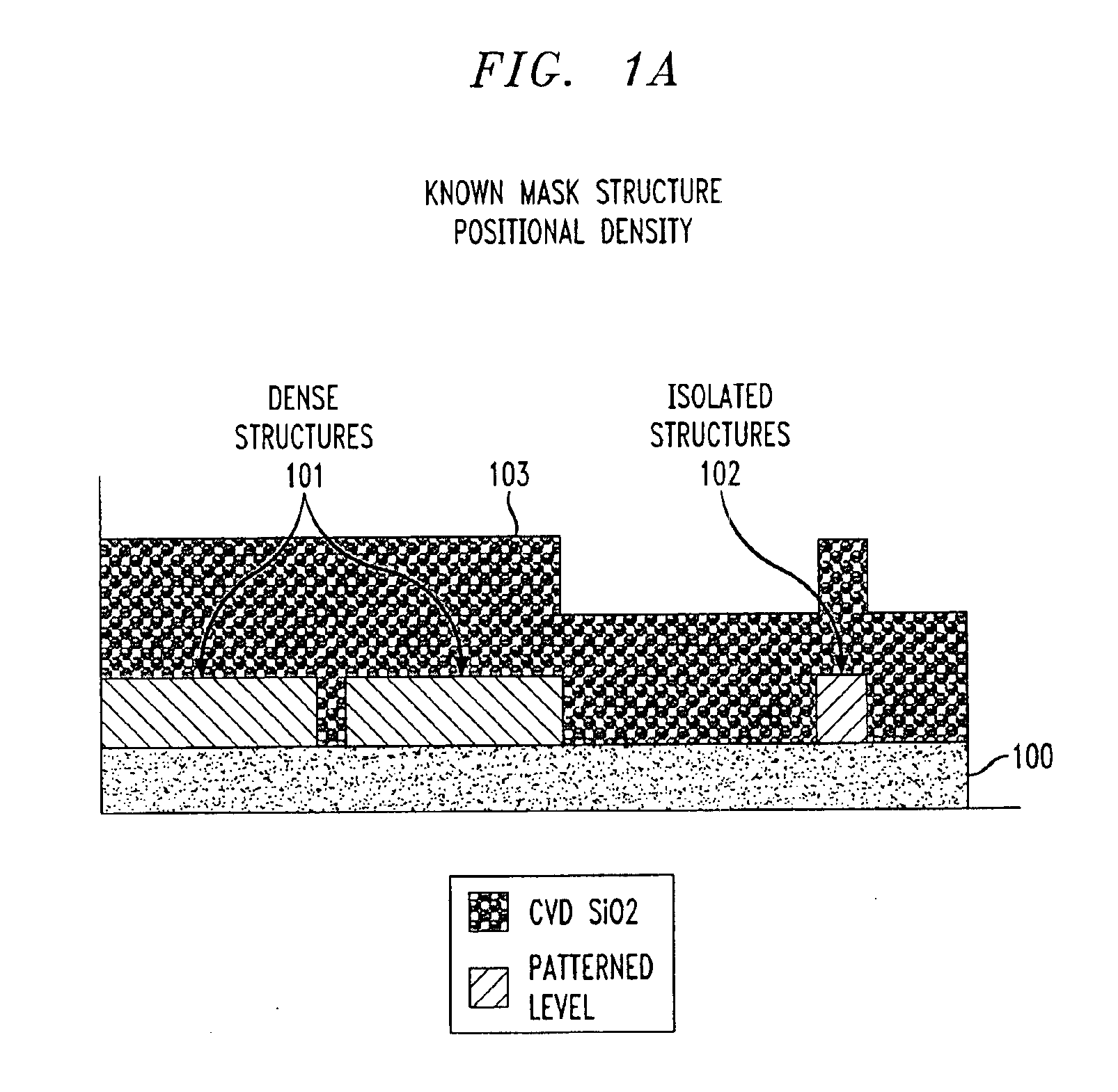
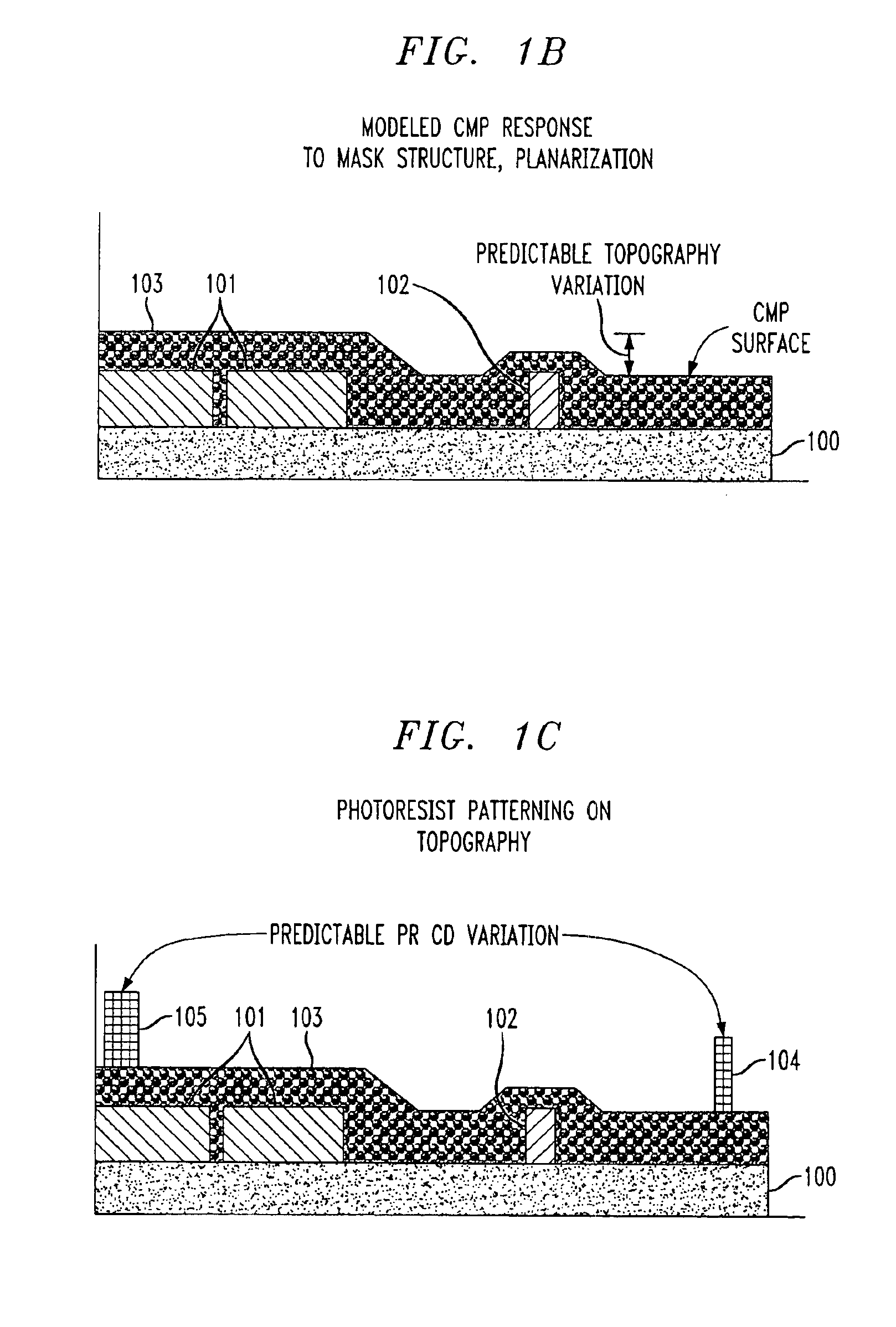
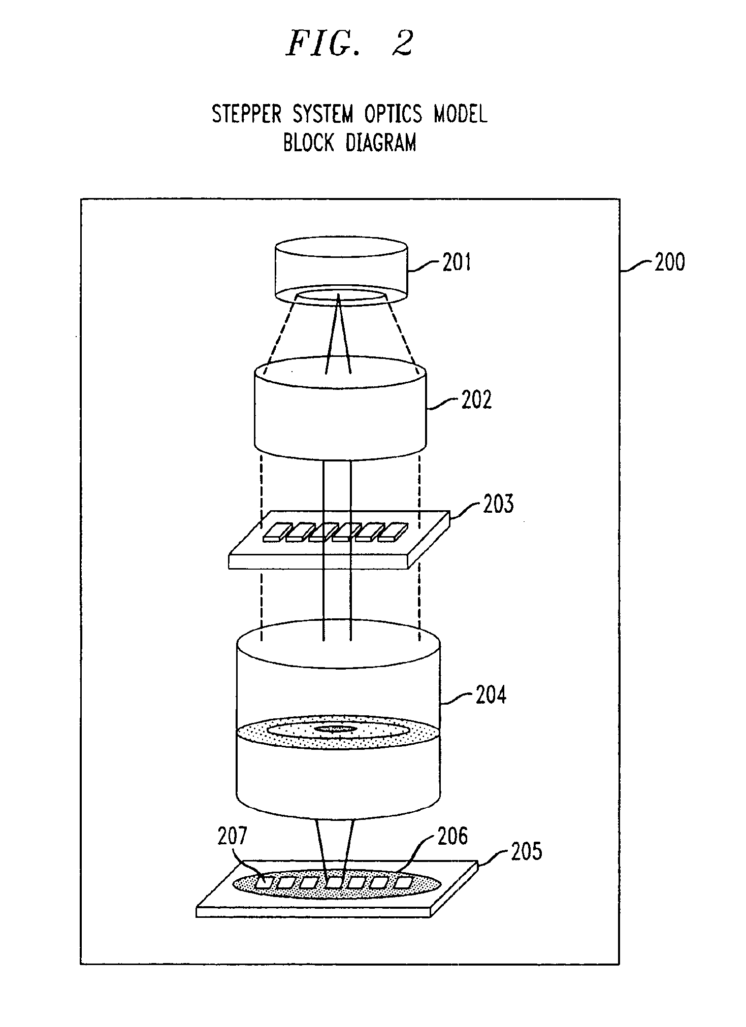
[0017]Semiconductor manufacturing includes a number of crucial processes performed on wafer lots, one of which is photolithography. As semiconductive materials are staged through these processes, it is essential to accurately perform photolithography since it determines device dimensions directly effecting quality, production yield, and manufacturing cost. Photolithography is also a critical process because it is iterated in a succession of exposure / processing steps to form a number of superimposed layers of insulators, conductors, and semiconductor materials.

[0018]Photolithographic processing occurs on a plurality or “lot” of wafers, which are fabricated as a batch. A representative photolithographic processing includes the following steps:[0019]Each wafer has material patterned on its surface using a photoresist patterning process (i.e., each wafer is coated with photoresist),[0020]Wafers are exposed to an energy source such as an ultraviolet light with a mask exposed onto the pho...


PUM


Abstract

A semiconductor manufacturing method analyzes topography variations in three dimensions for each photolithographic level and determines critical dimension (CD) bias compensation as inputs to mask layout creation. Accurate predictions of topography variation for a specific mask design are made at the die level using known pattern density and CMP planarization length characteristics for a specific pattern. Exhaustive characterization of the photoresist response to de-focus and mask bias is determined by artificially expanding loss of CD through focus. Mask compensation to an expanded range of focus over all lines and spaces is maintained within the specification. 3D mask density data is obtained to determine the height component at each pixel location in the die. The resulting 3D OPC model is then utilized for mask creation.

Description

FIELD OF THE INVENTION[0001]This invention relates in general to the field of semiconductor manufacturing. More particularly, this invention relates to a method for selective photolithographic mask correction on a semiconductor wafer surface compensating for 3D topographic non-uniformity.BACKGROUND OF THE INVENTION[0002]Photolithography is one of the most frequently employed semiconductor wafer processing techniques used to manufacturer integrated circuits (IC's). Photolithography comprises a process for forming a pattern (i.e., via photographic transfer) of complex circuit diagrams onto a semiconductor wafer surface for etching. These patterns are defined on the wafer in a succession of exposure and processing steps to form a number of superimposed layers. Manufacturing processes for IC devices depend upon extremely accurate reproduction of these patterns onto the wafer surface.[0003]During each photolithographic step, deviations are commonly introduced that distort the photomask i...

Claims


Application Information

Patent Timeline
IPC IPC(8): G03F1/14G03F7/00G03F1/00G03F1/36G03F7/207H01L21/027
CPCG03F1/144G03F7/70441G03F1/36G03F7/0035G03F1/70G03F7/20H01L21/027
Inventor JESSEN, SCOTTMCINTOSH, JOHN MARTINNAGEL, SCOTT M.
Owner BELL SEMICON LLC
Why Eureka
Try Eureka