Infrared radiating element and gas sensor using the same

A technology of infrared radiation and components, applied in the field of gas sensors, which can solve the problems of melting and easy damage of heat generators

Inactive Publication Date: 2006-12-27
MATSUSHITA ELECTRIC WORKS LTD
View PDF0 Cites 44 Cited by
  • Summary
  • Abstract
  • Description
  • Claims
  • Application Information

AI Technical Summary

Problems solved by technology

[0005] However, in the above-mentioned infrared radiation element having the microbridge structure, the heat generator is easily broken, and it may be melted by heat because the heat generator is linear and only both ends of the heat generator are supported by the supporting substrate write

Method used


Image

  • Infrared radiating element and gas sensor using the same
  • Infrared radiating element and gas sensor using the same
  • Infrared radiating element and gas sensor using the same

Examples


Embodiment Construction

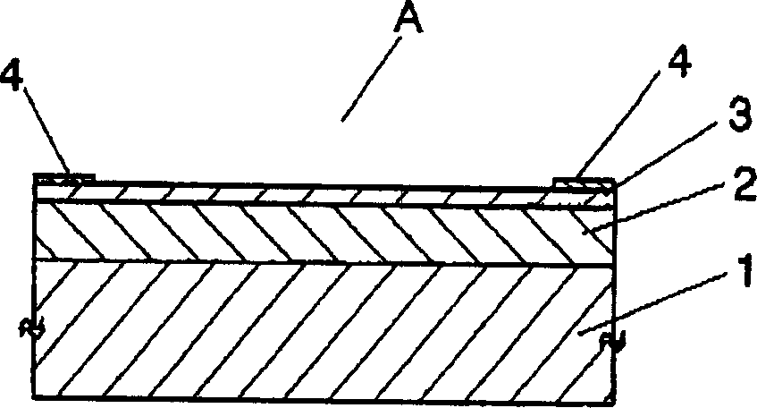
[0029] Hereinafter, the infrared radiation element (A) of the present invention will be described in more detail with reference to the accompanying drawings.

[0030] The infrared radiating element (A) of the present invention is an infrared radiating element that emits infrared rays from the heating layer 3 by energizing the heating layer 3 to heat the heating layer 3. In the infrared radiation element (A), the heat insulating layer 2 is formed on the surface of the semiconductor substrate 1 in the thickness direction (ie, figure 1 The heat-insulating layer 2 is porous and has a sufficiently smaller thermal conductivity than the semiconductor substrate 1. The heat-generating layer 3 is formed on the heat-insulating layer 2, and the heat-generating layer 3 is in the form of a thin layer (flat) and is higher than the heat-insulating layer. The layer 2 has greater thermal conductivity and greater electrical conductivity, and a pair of pads (electrodes) 4 for energization are formed...


PUM

PropertyMeasurementUnit
thicknessaaaaaaaaaa
thicknessaaaaaaaaaa
thicknessaaaaaaaaaa

Abstract

Disclosed is an infrared light emitting device (A) comprising a semiconductor substrate (1), a heat insulating layer (2) having a heat conductivity sufficiently lower that that of the semiconductor substrate (1) and formed on one surface of the semiconductor substrate (1) in the thickness direction, a lamellar heating layer (3) having a heat conductivity and electrical conductivity higher than those of the heat insulating layer (2) and formed on the heat insulating layer (2), and a pair of pads (4) formed on the heating layer (3) for electrical conduction. The semiconductor substrate (1) is composed of a silicon substrate. The heat insulating layer (2) and the heating layer (3) are composed of porous silicon layers having different porosities, and the porous silicon layer for the heating layer (3) has a lower porosity than that for the heat insulating layer (2). By using such an infrared light emitting device (A) as the infrared radiation source in a gas sensor, there can be realized an infrared radiation source having a prolonged life.

Description

Technical field [0001] The invention relates to an infrared radiation element and a gas sensor using the infrared radiation element. Background technique [0002] Various types of analyzers using infrared radiation sources have been provided, such as infrared gas analyzers. The typical infrared radiation source used in this type of analyzer is a halogen lamp. However, the halogen lamp is large and has a short life span, so it is difficult to use it for a small gas sensor that uses infrared light to detect gas. [0003] Therefore, as an infrared radiation source that can be miniaturized, infrared radiation elements formed by micromachining technology have been developed in many places (for example, see Japanese Unexamined Patent Publication No. 9-153640 ([0027]-[0028] paragraphs). , figure 2 ), Japanese Unexamined Patent Publication No. 2000-236110 ([0017]-[0019] paragraphs, figure 1 with 2 ) And Japanese Unexamined Patent Publication No. 10-294165 (paragraphs [0014]-[0015], fig...

Claims


Application Information

Patent Timeline
Patent Type & Authority Applications(China)
IPC IPC(8): H01K1/04H05B3/10G01N21/01
Inventor 栎原勉滨田长生明渡甲志北村启明福岛博司菰田卓哉幡井崇
Owner MATSUSHITA ELECTRIC WORKS LTD
Why Eureka
Try Eureka