

Semiconductor light-emitting device and method for manufacturing same
A technology for a light-emitting element and a manufacturing method, which can be applied to semiconductor devices, semiconductor lasers, electrical components, etc., can solve problems such as peeling and poor adhesion, and achieve the effects of suppressing invalid light emission and improving external quantum efficiency.
- Summary
- Abstract
- Description
- Claims
- Application Information
AI Technical Summary
Problems solved by technology
Method used
Image

Examples
Embodiment Construction
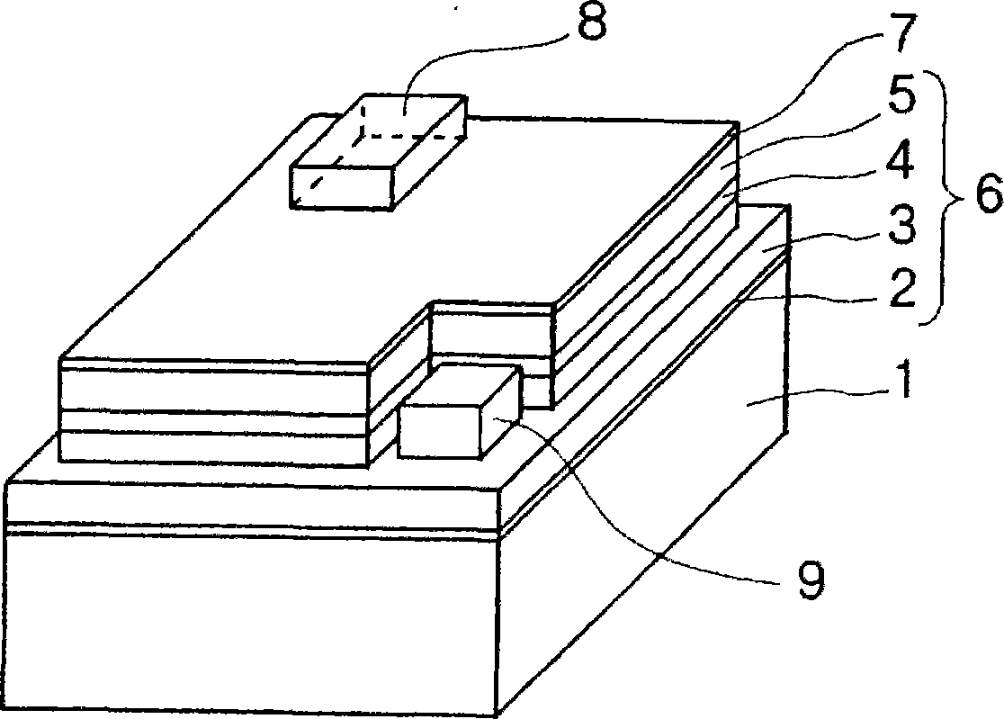
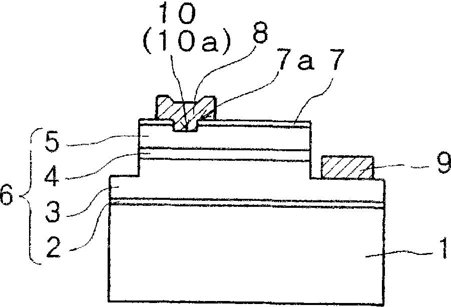
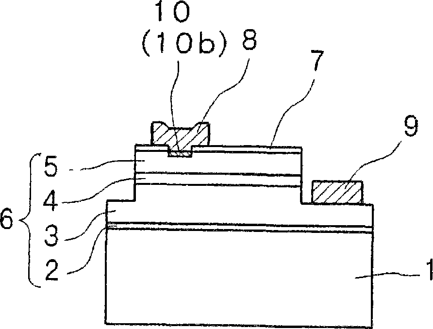
[0034] Next, the semiconductor light-emitting element of the present invention and its manufacturing method will be described with reference to the drawings. The semiconductor light-emitting device of the present invention, an explanatory diagram of a perspective view and a cross-sectional view of an embodiment thereof, is shown in FIG. In the laminated portion 6 , a light-transmitting conductive layer 7 is provided on the surface of the semiconductor laminated portion 6 . A part of the translucent conductive layer 7 is removed, and an upper electrode (electrode pad) 8 is provided in contact with the exposed surface of the semiconductor laminate 6 and the translucent conductive layer 7 . In the present invention, a structure is formed in which a portion of the translucent conductive layer 7 is removed, and a current suppressing mechanism 10 (10a) is provided on the surface of the semiconductor lamination layer 6 exposed from the opening 7a, thereby forming a secure upper elect...
PUM
 Abstract
Description
Claims
Application Information