Method and system for designing optical shield layout and producing optical shield pattern

A mask and pattern technology, applied in the field of lithography process, to achieve the effect of wide utilization value, product structure improvement, and improvement of image distortion

A mask and pattern technology, applied in the field of lithography process, to achieve the effect of wide utilization value, product structure improvement, and improvement of image distortion

CN1904726AActive Publication Date: 2007-01-31TAIWAN SEMICON MFG CO LTD

Image

  • Method and system for designing optical shield layout and producing optical shield pattern
  • Method and system for designing optical shield layout and producing optical shield pattern
  • Method and system for designing optical shield layout and producing optical shield pattern

Examples


Embodiment Construction

[0072] In order to further explain the technical means and effects of the present invention to achieve the intended purpose of the invention, the method and system for designing the layout of the mask and generating the pattern of the mask according to the present invention will be described in detail below in conjunction with the accompanying drawings and preferred embodiments. Embodiments, methods, steps, structures, features and effects thereof are described in detail below.

[0073] This disclosure is related to the field of optics or lithography. To illustrate the present disclosure, several specific examples and types of systems, formulations, patterns, and substrates are described and discussed below. It should be appreciated, however, that these specific examples are intended to teach broader inventive concepts, and those skilled in the art can readily apply the teachings of this disclosure to other related fields.

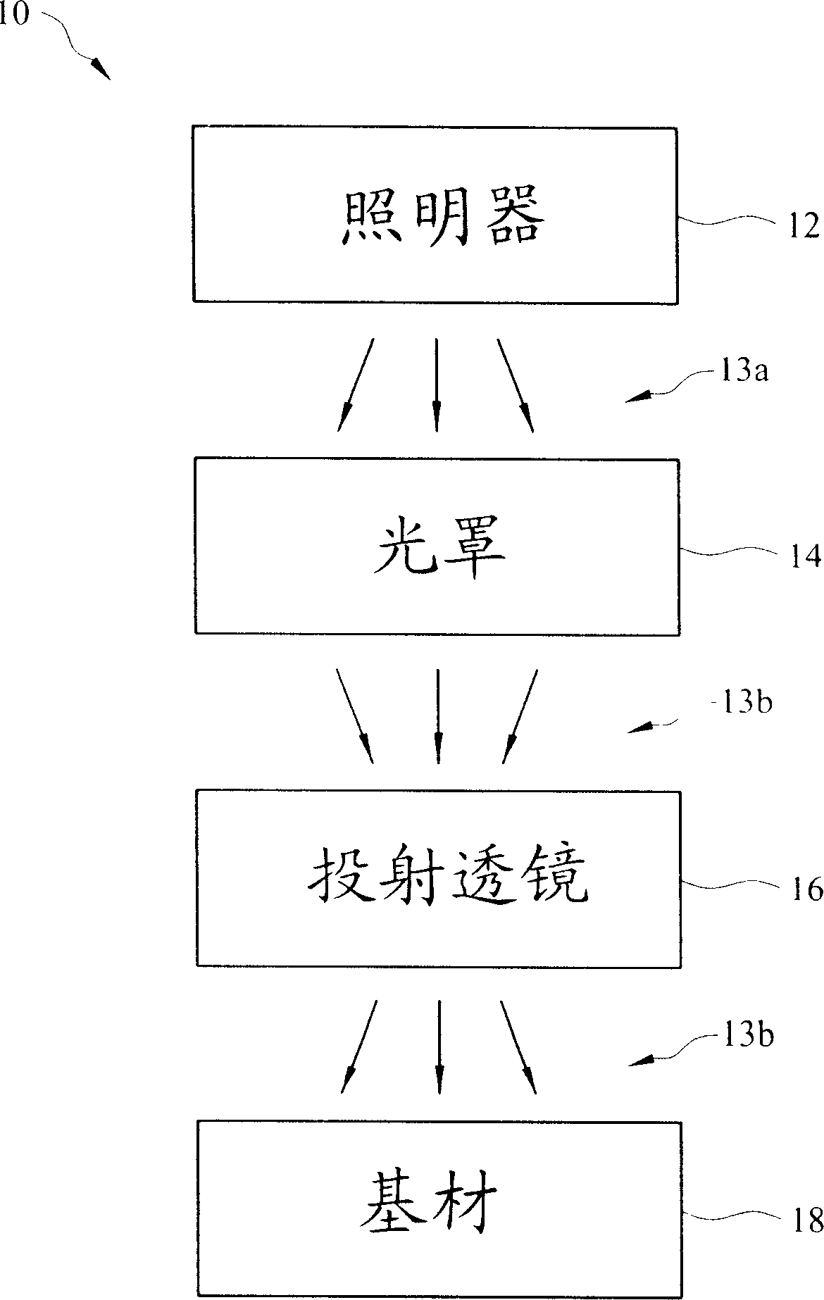
[0074] see figure 1 As shown, semiconductor lithog...


PUM


Abstract

The present invention relates to a method and system for designing a mask layout and generating a mask pattern. The method includes using a plurality of pixels to represent the mask layout, wherein each pixel has a mask transparency coefficient. A control parameter is initialized and a representation of the mask layout is generated. This method uses a cost function and a Boltzmann probability function (Boltzmann Probability Function) to decide whether to accept the representative of the mask layout, wherein the cost function is related to the mask layout and the target substrate pattern, and the Boltzmann probability function is related to The cost function is related to the control parameters. The step of generating a representative of the reticle layout and the step of accepting a representative of the reticle layout are repeated until the reticle layout is stabilized. Reduce this control parameter according to the annealing program. The steps of generating a representative of the reticle layout, determining, reworking, and reducing the control parameters are repeated until the reticle layout is optimized.

Description

technical field [0001] The present invention relates to a lithography process, in particular to a method and system for designing a mask layout and generating a mask pattern used in a lithography process for manufacturing a semiconductor integrated circuit. Background technique [0002] Lithography refers to a technique that uses a photon beam to project a pattern on a photomask onto a substrate for imaging. Taking the manufacture of semiconductor integrated circuits as an example, with the miniaturization of the size of circuit components, the lithography process needs to have the ability to form images with the smallest feature size on the semiconductor wafer. [0003] Due to the low-pass filtering effect of the lithography optical system, the diffraction from the mask and the lithography system can cause image distortion and deterioration. For example, right-angled corners on a reticle may appear as rounded corners on a semiconductor wafer. The degree of image distortio...

Claims


Application Information

Patent Timeline
31 Jan 2007
Publication
CN1904726A
IPC
G03F1/08; G03F7/00; H01L21/00
CPC
G03F1/144; G03F1/36
Inventors
周硕彦; 许照荣