Supercharge Your Innovation With Domain-Expert AI Agents!

Memory array module

A memory array and memory chip technology, which is applied in the direction of instruments, electrical digital data processing, digital data processing parts, etc., can solve the problems of high personnel costs, empty welding, and inability to meet the processing process, etc.

Inactive Publication Date: 2007-01-31
OPTIMUM CARE INT TECH
View PDF0 Cites 1 Cited by
  • Summary
  • Abstract
  • Description
  • Claims
  • Application Information

AI Technical Summary

Problems solved by technology

[0004] (1) The memory chip A2 used in the prior art is welded on the substrate A1 by welding. If any memory chip A2 is damaged or malfunctions, the substrate A1 must be removed from the socket B1 for reuse. In the way of high-temperature melting, each pin of the memory chip A2 is desoldered, and the desoldering operation is performed, and the damaged memory chip A2 can be removed from the substrate A1. After replacing the new memory chip A2, high-temperature soldering must be used again. In this way, the memory chip A2 is re-soldered on the substrate A1. However, the general memory chip A2 has developed towards the trend of miniature, lightweight and high-density packaging. In contrast, the pin spacing of the memory chip A2 is more dense, so , making it more difficult for the memory chip A2 to perform desoldering and reflow operations, and high-temperature operations are particularly likely to affect other peripheral memory chips A2, causing other memory chips A2 to be easily damaged or malfunctioned due to high temperature overheating or inadvertent collision. This in turn increases the difficulty of maintenance operations
[0005] (2) No matter the desoldering or reflowing operation of the memory chip A2 used in the prior art, it must be done manually, which makes the overall operation quite cumbersome and inconvenient, and the soldering operation must be performed by professional practitioners, so The required personnel costs are also quite high, thereby increasing the overall maintenance cost, and the manual soldering operation is also likely to lead to improper soldering (such as empty soldering, overheating, poor contact, etc.), which increases the defect rate of the memory chip A2 during maintenance. , must consume more additional material costs
[0006] (3) The memory module A and the computer motherboard B used in the prior art must be manufactured separately, so that the production of the memory module A and the parts configuration on the computer motherboard B are all different processing procedures, but the memory module A and the computer mainframe The relationship between board B, whether it is in terms of specifications or hardware, must be able to cooperate with each other before they can be used. However, each time memory module A and computer motherboard B are processed, they can only be processed separately for a single item, so that The entire processing process must be carried out in sections and sub-items. In this way, the processing process of the overall consistent manufacturing cannot be met, and the memory module A and the computer motherboard B cannot achieve the purpose of mass production at the same time, which will only increase the overall processing. Time, and troubles and troubles caused by production operations

Method used


Image

  • Memory array module
  • Memory array module
  • Memory array module

Examples


Embodiment Construction

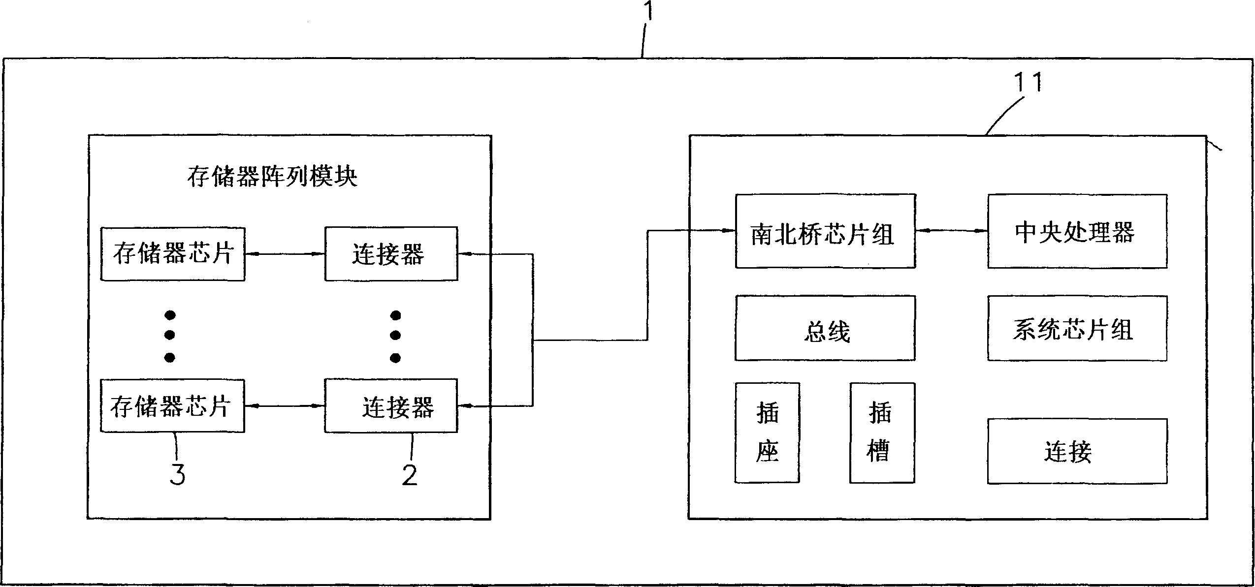
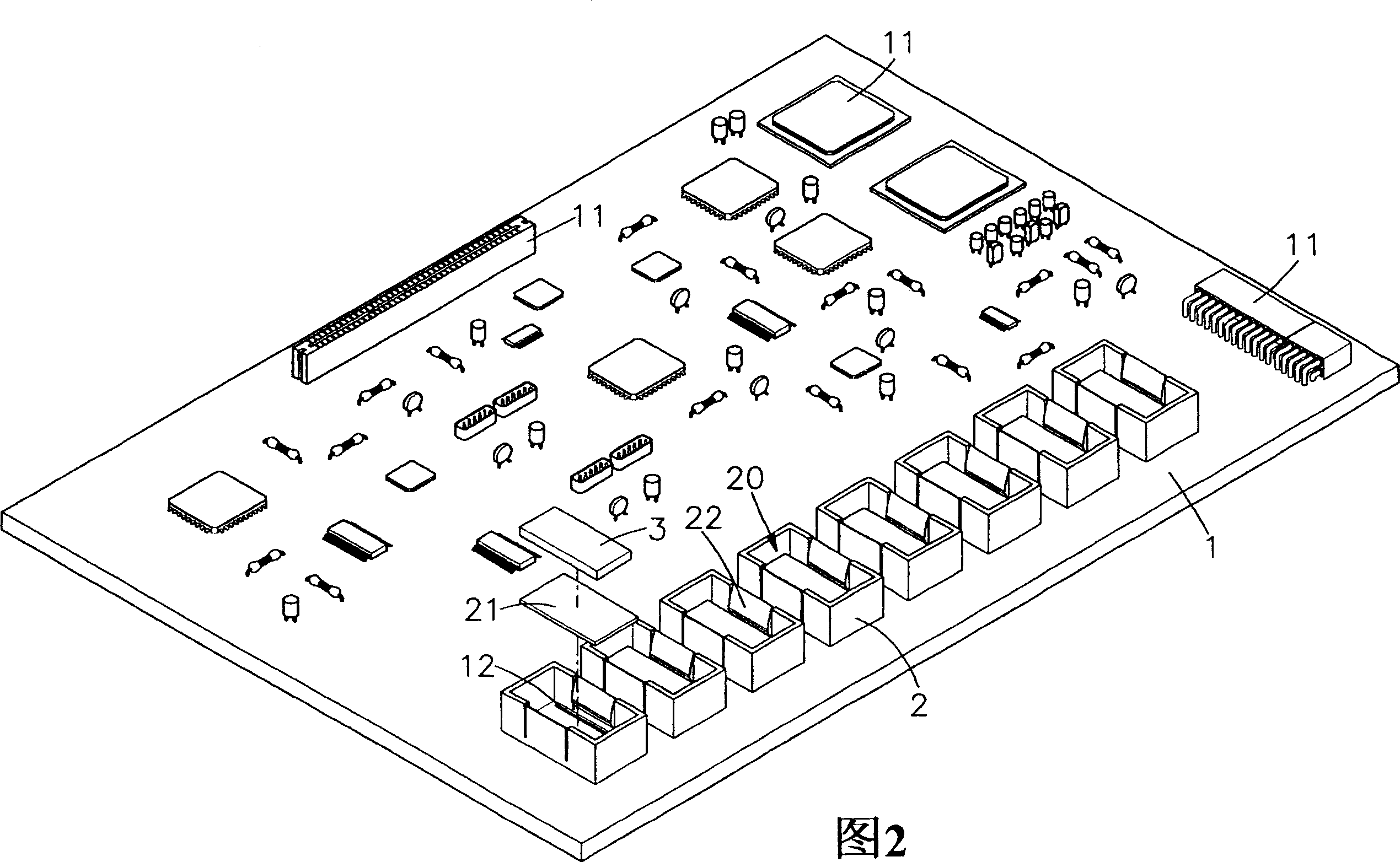
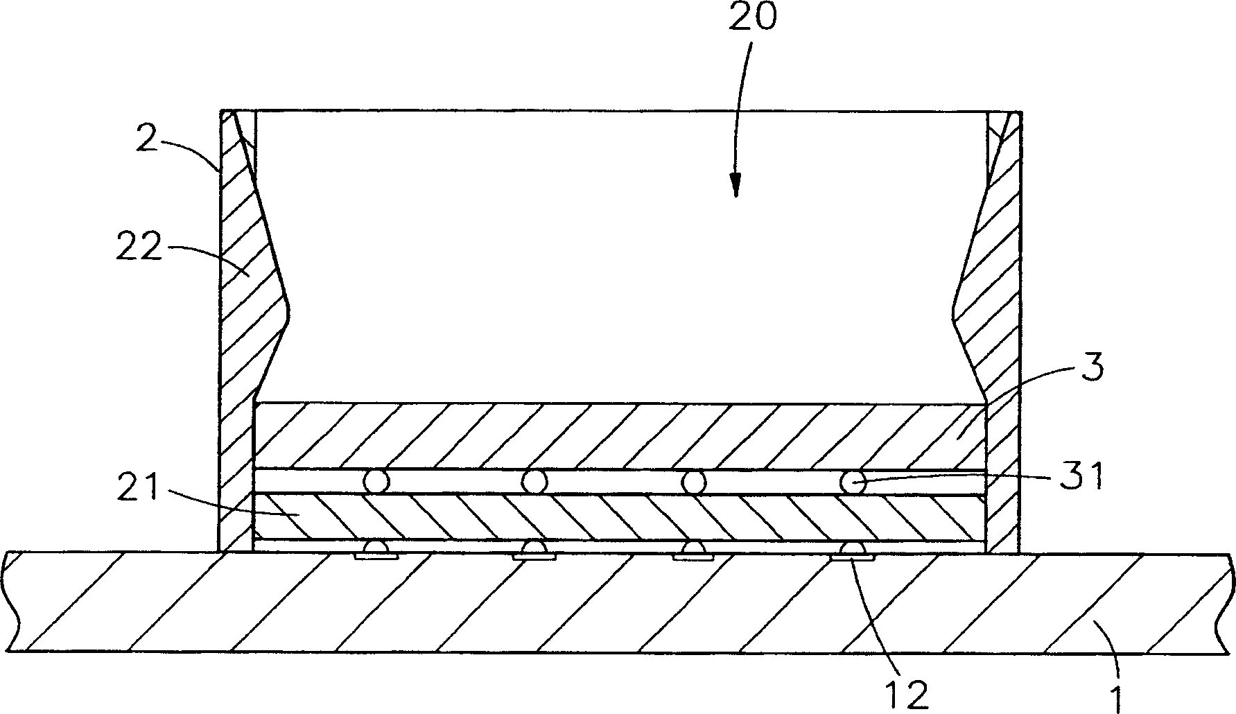
[0045] see figure 1 As shown, it is a schematic block diagram of the present invention. It can be clearly seen from the figure that the memory array module of the present invention is mainly provided with circuit contacts 12 and related electronic parts 11 on the motherboard 1, and its electronic parts 11 can be system Chipset, central processing unit, bus, slot, socket or connection port, etc., and two or more connectors 2 are additionally arranged on the motherboard 1, wherein each connector 2 provides a memory chip 3 on the In the welding state, it is combined and positioned, and the memory chip 3 can be electrically connected to the preset circuit contact 12 on the main board 1. Therefore, when the main board 1 is processed and etched with the circuit contact 12 in the present invention, the connector 2 can be connected simultaneously. The required circuit contacts are arranged on the main board 1 to simplify the overall processing flow of the main board 1 and effectively ...


PUM


Abstract

The invention relates to a memory array module that sets two or more linkers, circuitry contact and relative electric components on host computer. The linkers supplies combination location under solderless state for memory and make memory chip electrically connecting to circuitry contact. When the memory at linker place needs to replace or mend, high temperature operation would be avoided and the damaging to other component would be also avoided. It could also take further simplifying replacement or changing other memory chip of different capacity. The effect of easy to mend and low cost would be also realized.

Description

technical field [0001] The invention provides a memory array module, especially a memory array module which utilizes two or more than two connectors on the mainboard of a computer to provide memory chips that can be combined and positioned without welding, and can easily replace the memory chips. Background technique [0002] With the advent of the high-tech era, more and more electronic technology products are flooding around the living environment, providing people with advanced enjoyment in all aspects of life, work, leisure and entertainment. Among various electronic technology products, the The computer has the most direct relationship with people's life. It can provide the most convenient information in people's life or work. Among them, the memory module plays an extremely important role in the computer. Without it, the computer cannot be turned on, and the peripheral device cannot transmit data to the processor, and the processor cannot receive information from the p...

Claims


Application Information

Patent Timeline
Patent Type & Authority Applications(China)
IPC IPC(8): G06F1/00G06F13/00
Inventor 连世雄
Owner OPTIMUM CARE INT TECH
Features
  • R&D
  • Intellectual Property
  • Life Sciences
  • Materials
  • Tech Scout
  • Unparalleled Data Quality
  • Higher Quality Content
  • 60% Fewer Hallucinations
Learn More