Magnetic memory device

A magnetic storage device and storage unit technology, applied in static memory, digital memory information, information storage, etc., can solve the problems of increased resistance value and parasitic capacitance, and longer information readout time, and achieve high-speed readout effect

CN1905061AInactive Publication Date: 2007-01-31TDK CORPARATION
1 Cites 4 Cited by

Patent Information

Authority / Receiving Office
CN · China
Patent Type
Applications(China)
Current Assignee / Owner
Publication Date
2007-01-31
Estimated Expiration
Not applicable · inactive patent

Smart Images

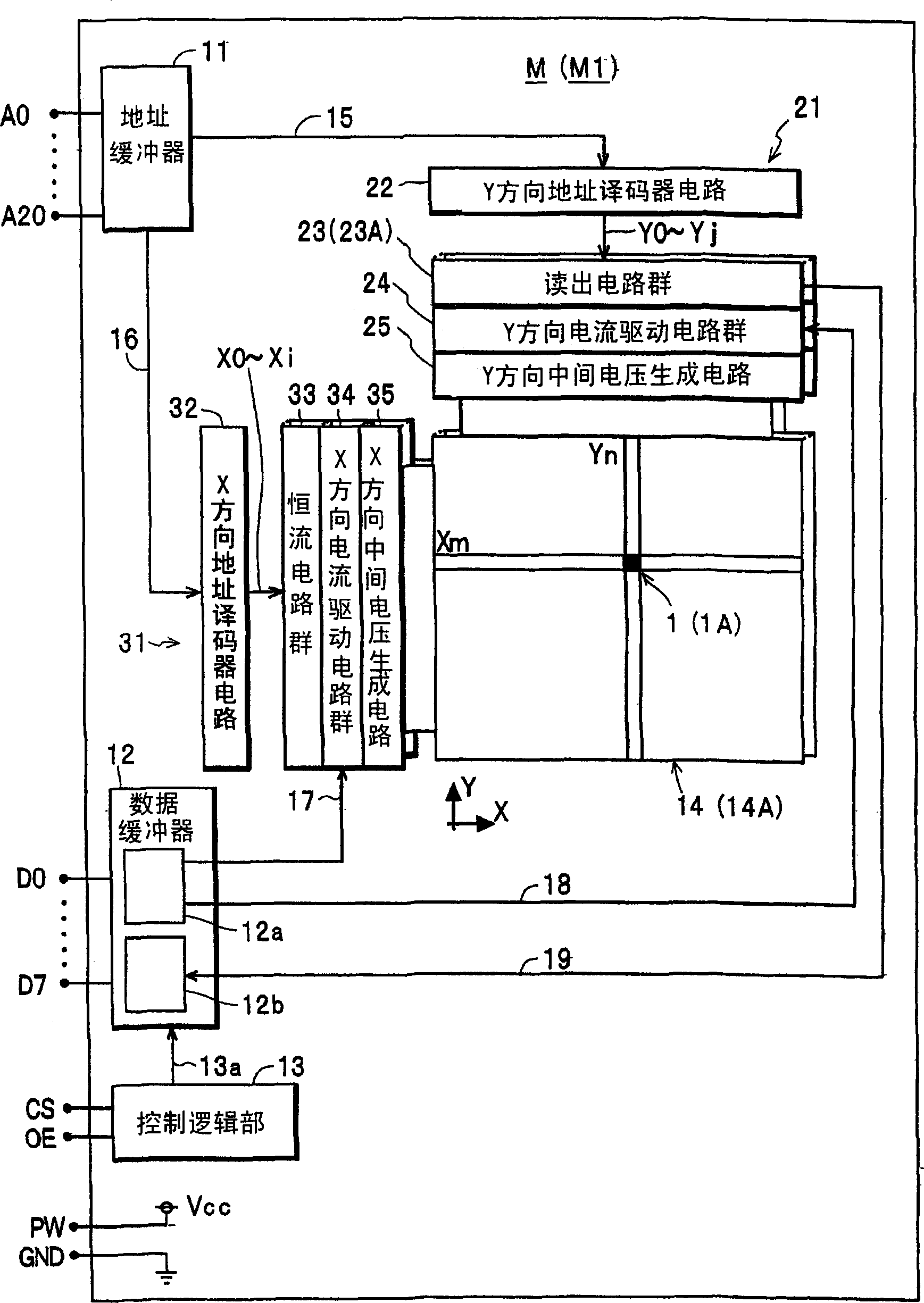
  • Figure 1
    Figure 1
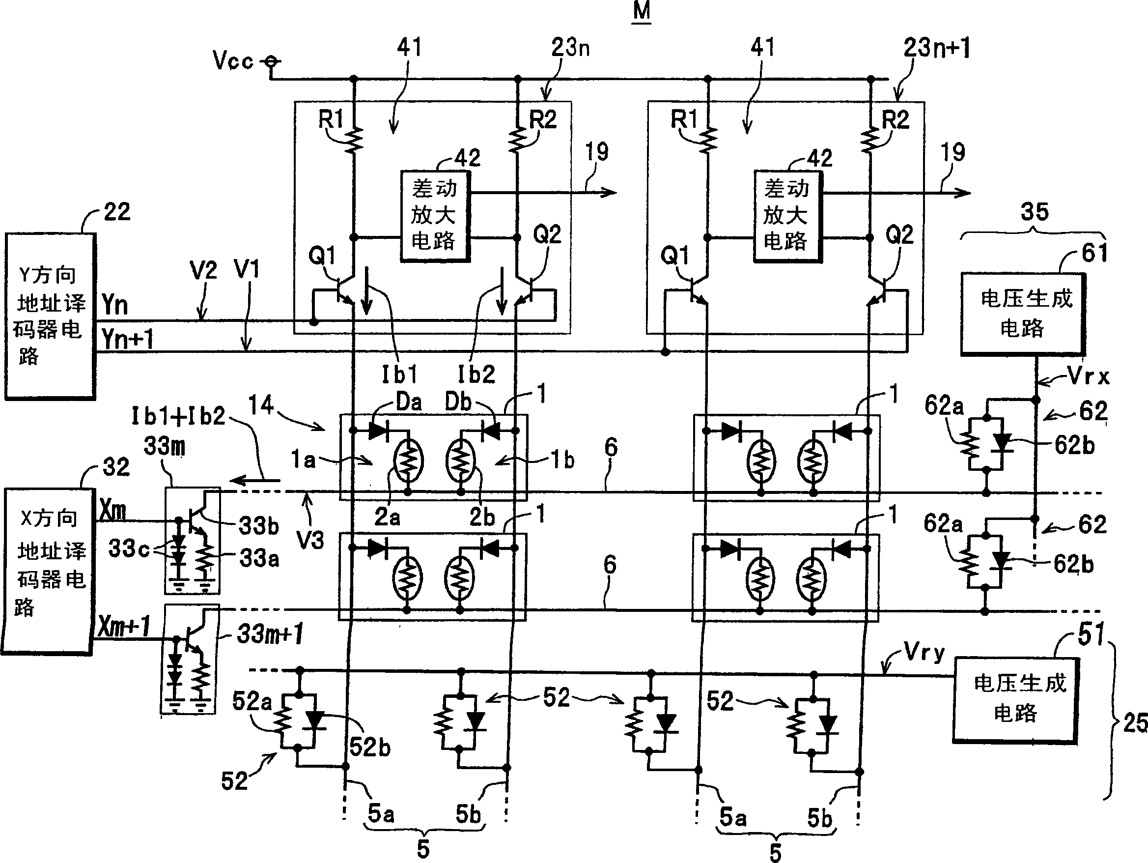
  • Figure 2
    Figure 2
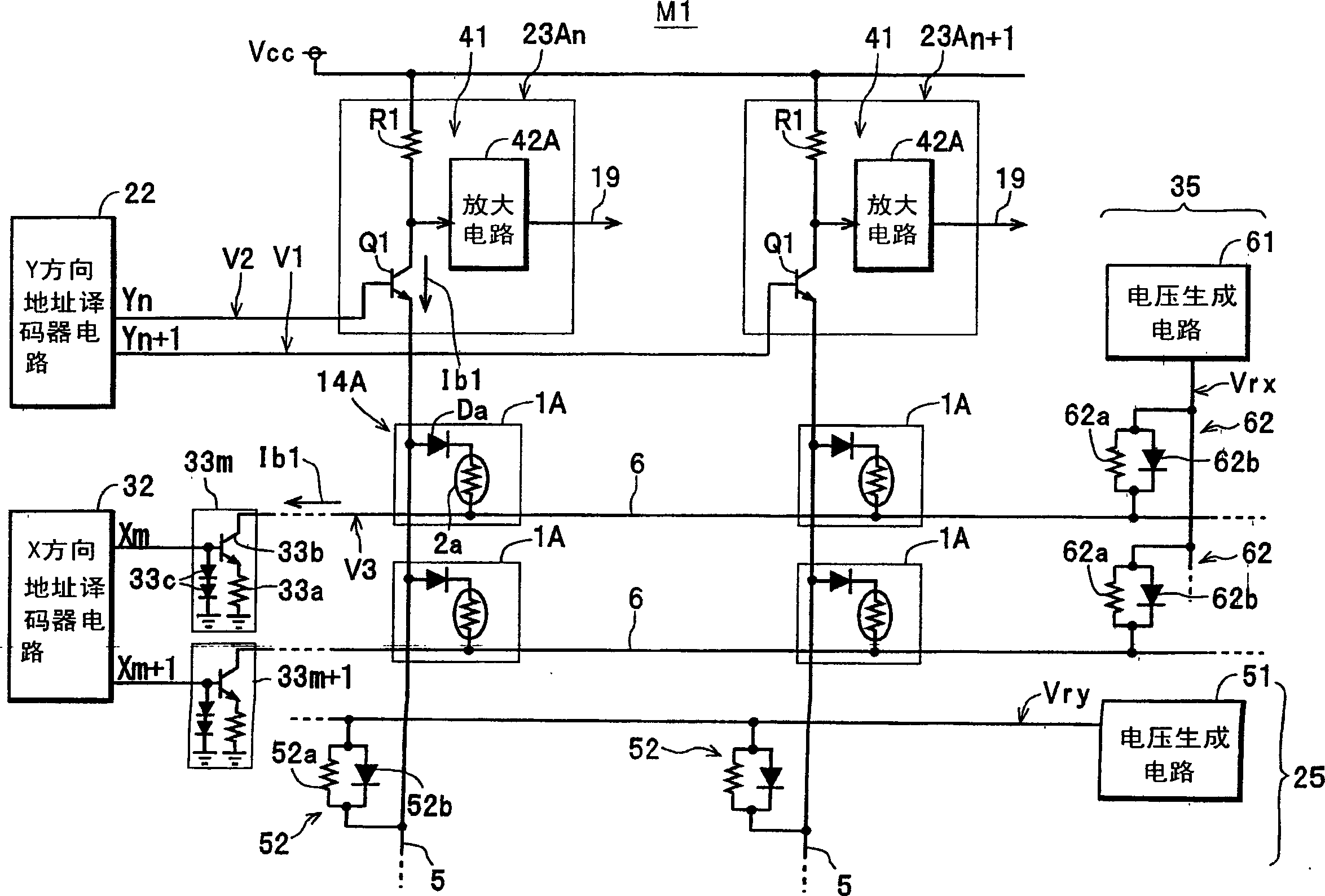
  • Figure 3
    Figure 3
Patent Text Reader

Abstract

The invention provides a magnetic memory device capable of reading information at high speed. The device is equipped with a plurality of storage cells 1 arranged in two-dimensional array; a plurality of read bit lines 5 and a plurality of read word lines 6 for supplying read current Ib1, Ib2 for reading the information from first power supply (supply voltage Vcc) to each of the storage cells 1; a medium voltage generation circuit 25 of Y direction, connected to a part of the read bit line 5, for impressing the medium voltage Vry, lower than the supply voltage Vcc, to the read bit line 5; and a medium voltage generation circuit 35 of X direction, connected to the part of the read word line 6, for impressing the medium voltage Vrx, lower than supply voltage Vcc, to the read word line 6.
Need to check novelty before this filing date? Find Prior Art

Description

technical field

[0001] The present invention relates to a magnetic memory device capable of recording and reading information with a memory unit including a magnetoresistance effect display body. Background technique

[0002] As such a magnetic memory device, there is known a magnetic memory device disclosed in Japanese Unexamined Patent Publication No. 2004-119638 already proposed by the applicant of the present application. The magnetic storage device is a magnetic random access memory (hereinafter also referred to as "MRAM: Magnetic Random Access Memory"), such as Figure 5 As shown, a plurality of memory cells 1 are respectively arranged in the word line direction (X direction) and a memory cell group 14 in the bit line direction (Y direction), and a plurality of read word lines 6 are arranged in the X direction, so that Two lines form a set of a plurality of read bit lines 5 arranged in the Y direction, forming a matrix as a whole. Each memory cell 1 is constituted by ...

Examples

Embodiment Construction

[0033] Hereinafter, the best mode of the magnetic memory device of the present invention will be described with reference to the drawings.

[0034] First, refer to figure 1 , 2 The configuration of the magnetic memory device M of the present invention will be described.

[0035] Such as figure 1 As shown, the magnetic storage device M includes an address buffer 11 , a data buffer 12 , a control logic unit 13 , a storage cell group 14 , a Y direction drive control circuit unit 21 , and an X direction drive control circuit unit 31 . In this case, the Y-direction drive control circuit unit 21 has a Y-direction address decoder circuit 22 , a readout circuit group 23 , a Y-direction current drive circuit group 24 , and a Y-direction intermediate voltage generation circuit 25 . On the other hand, the X-direction drive control circuit unit 31 has an X-direction address decoder circuit 32 , a constant current circuit group 33 , an X-direction current drive circuit group 34 , and ...