Film transistor array substrate and mfg. method thereof

A technology of thin film transistors and array substrates, applied in the field of thin film transistor array substrates and its production, can solve the problems of increasing the difficulty of manufacturing processes, affecting the pass rate of manufacturing processes, and high production costs, so as to reduce the number of photomask manufacturing processes and manufacture The process is simple and the effect of improving the aperture ratio

Active Publication Date: 2007-01-31
AU OPTRONICS CORP
View PDF1 Cites 8 Cited by
  • Summary
  • Abstract
  • Description
  • Claims
  • Application Information

AI Technical Summary

Problems solved by technology

[0005] It is worth noting that it is known that the manufacturing method of the TFT array substrate requires at least eight photomask manufacturing processes, the steps are complicated and the production cost is relatively high.
In addition, since a contact window with a high aspect ratio needs to be formed in a thick film layer such as a color filter layer and a flat layer to connect the pixel electrode and the source / drain electrode, it relatively increases the difficulty of the manufacturing process and indirectly Affect the qualification rate of manufacturing process

Method used


Image

  • Film transistor array substrate and mfg. method thereof
  • Film transistor array substrate and mfg. method thereof
  • Film transistor array substrate and mfg. method thereof

Examples


Embodiment Construction

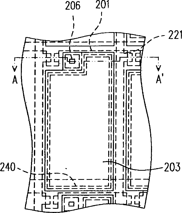
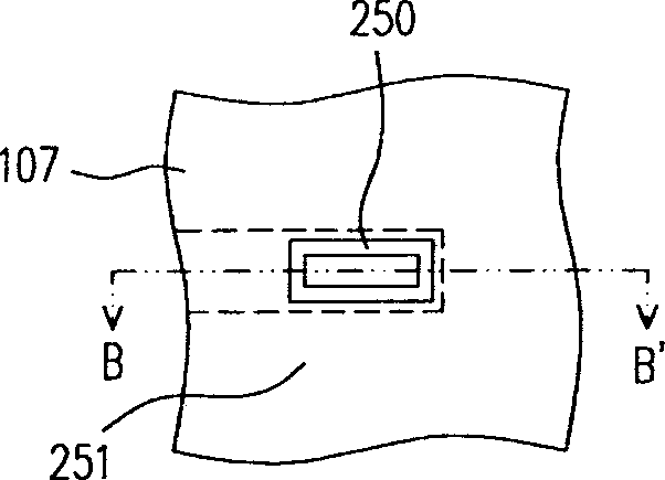
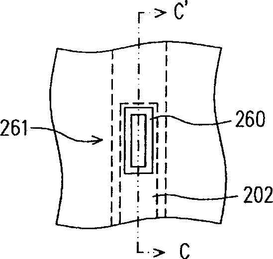
[0081] Figure 3A-3G The sequence is a top view of a manufacturing method of a thin film transistor array substrate according to a preferred embodiment of the present invention, and Figure 4Aa-4Ad ~ Figure 4Ga-4Gd are shown in sequence Figure 3A-3G The A-A' section, the B-B' section, the C-C' section and the D-D' section.

[0082] First, if Figure 3A and Figure 4Aa-4Ad As shown, a substrate 302 is provided, such as a transparent substrate made of glass, and the substrate 302 is divided into a plurality of sub-pixel regions 302a. Next, a plurality of film layers are sequentially formed on the substrate 302 , including a first conductive layer 312 , an insulating layer 314 and a channel layer 316 . Wherein, the first conductive layer 312 may be a metal stack composed of titanium / aluminum / titanium (Ti / Al / Ti), and the method of forming the first conductive layer 312 is, for example, sequentially through sputtering. Metal layers such as titanium / aluminum / titanium are depos...


PUM

PropertyMeasurementUnit
thicknessaaaaaaaaaa
thicknessaaaaaaaaaa
thicknessaaaaaaaaaa

Abstract

The invention discloses a thin film transistor (TFT) array substrate and the making method thereof. And the making method only needs six or even less photo-mask manufacturing processes to be able to make a TFT array substrate integrated with color filter pattern. Therefore, the making method is relatively simple to implement and has lower production cost. Besides, the making method need not form contact windows in thicker films, such as flat layer or color filter layer, to connect pixel electrodes with sources / drains, thus able to effectively reduce the difficulty of the manufacturing process.

Description

technical field [0001] The present invention relates to a thin film transistor array substrate and a manufacturing method thereof, and in particular to a thin film transistor array substrate with a color filter on array (COA) formed on an element array and a manufacturing method thereof. Background technique [0002] Liquid crystal displays have the advantages of high image quality, small size, light weight, low voltage drive, low power consumption, and wide application range. Therefore, they have replaced cathode ray tubes (Cathode Ray Tube, CRT) and become the mainstream of the new generation of displays. A traditional liquid crystal display panel is composed of a color filter substrate (Color Filter), a thin film transistor array substrate (TFT Array Substrate), and a liquid crystal layer arranged between the two substrates. In order to improve the resolution of the panel and the aperture ratio of the pixels, and to avoid the alignment error when the color filter substrat...

Claims


Application Information

Patent Timeline
Patent Type & Authority Applications(China)
IPC IPC(8): H01L21/84H01L21/768H01L27/12H01L23/522G02F1/1362
Inventor 游伟盛陈建宏
Owner AU OPTRONICS CORP
Why Eureka
Try Eureka