

Developing treatment apparatus and developing treatment method
A technology of processing device and processing unit, which is applied in the direction of electrical components, semiconductor/solid-state device manufacturing, circuits, etc., which can solve problems such as developing defects, uneven developing, and uneven concentration of developer, so as to suppress the generation of particles and stabilize the developer , Yield improvement effect
- Summary
- Abstract
- Description
- Claims
- Application Information
AI Technical Summary
Problems solved by technology
Method used
Image

Examples
Embodiment Construction
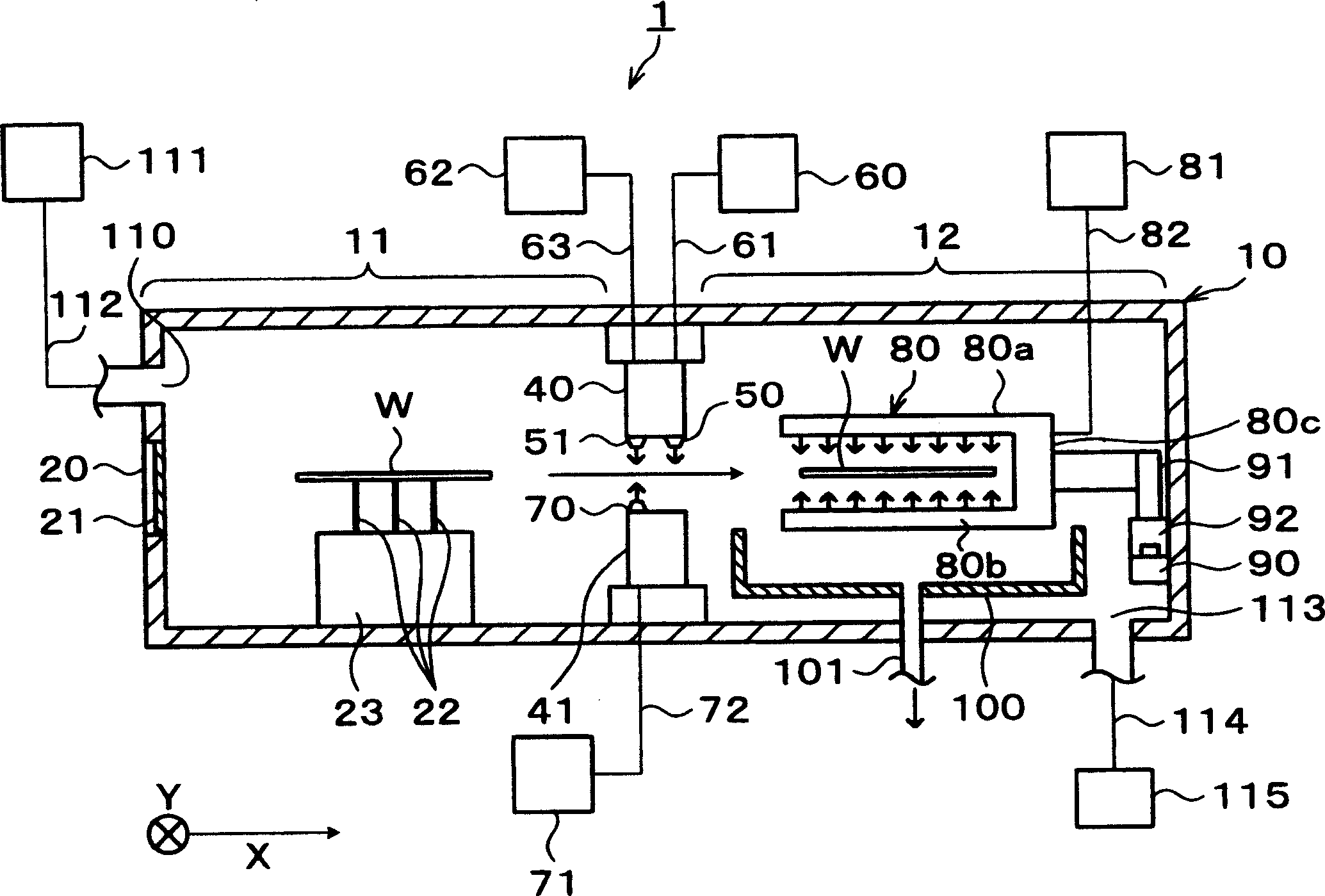
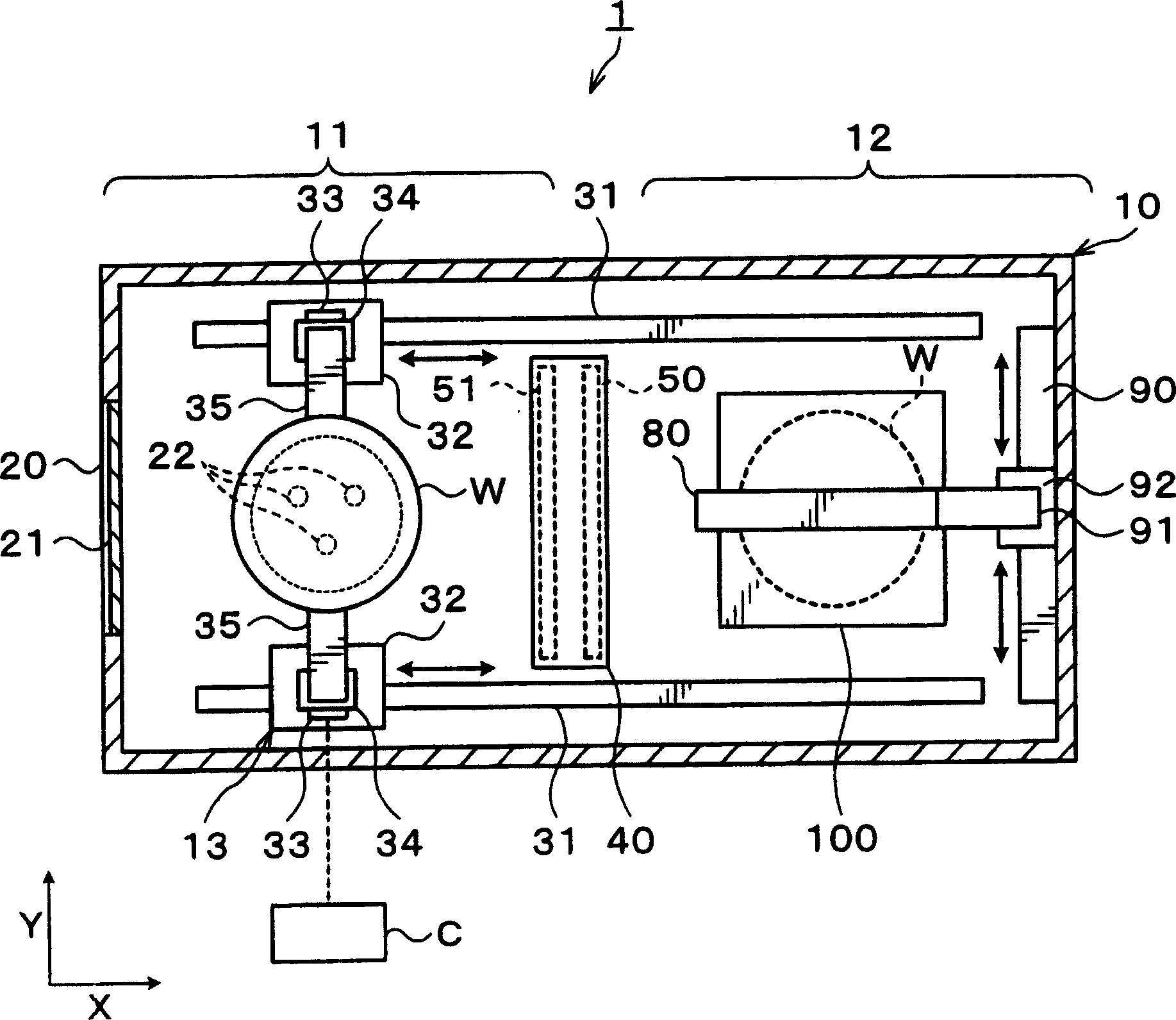
[0038] Next, the best mode for carrying out the present invention will be described. figure 1 It is a longitudinal cross-sectional explanatory view showing a schematic configuration of the development processing apparatus 1 according to the present embodiment. figure 2 It is an explanatory cross-sectional view schematically showing the configuration of the development processing device 1 .
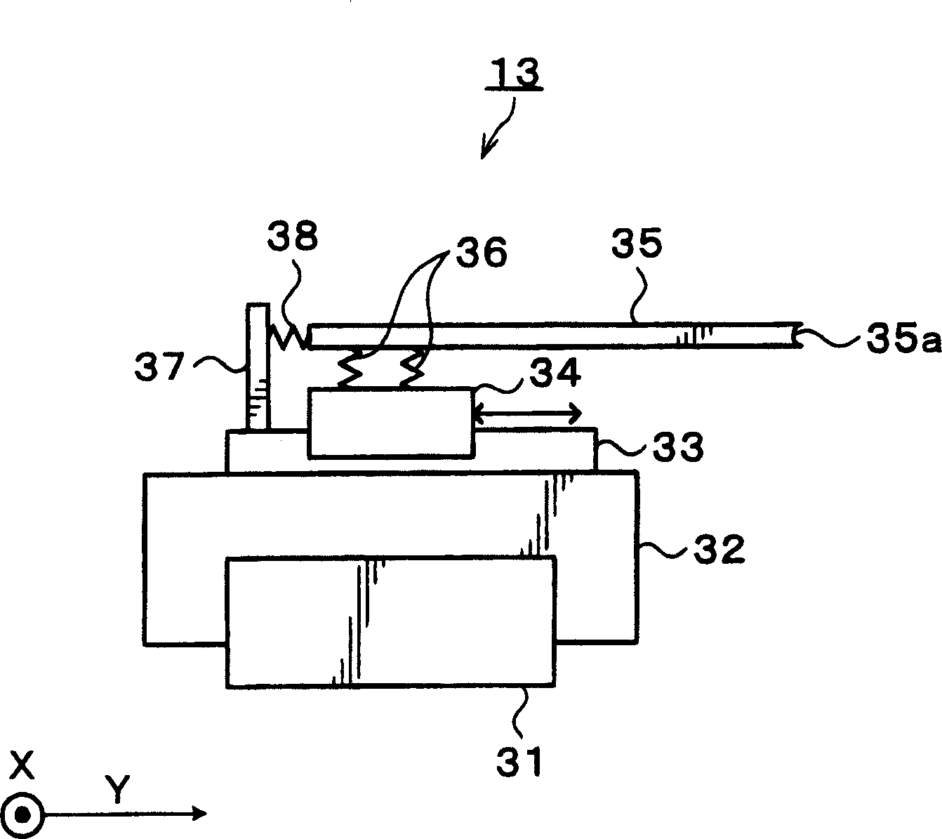
[0039] The development processing device 1 has, for example, figure 1 A closed processing vessel 10 is shown. The processing container 10 is shaped in the X direction ( figure 1 The left and right directions) are formed in an approximately rectangular parallelepiped shape. In the processing container 10 , a transfer unit 11 for transferring the wafer W to the outside and a development processing unit 12 for developing the wafer W are arranged in line in the X direction. In addition, if figure 2 As shown, the processing container 10 is provided with a transport mechanism 13 for transpo...
PUM
 Abstract
Description
Claims
Application Information