Analog-to-digital converter with noise compensation in cmos image sensor

一种图像传感器、数字转换器的技术,应用在模数转换器、模/数转换、物理参数补偿/预防等方向,能够解决功率噪声、图像失真等问题

Inactive Publication Date: 2007-02-07
SAMSUNG ELECTRONICS CO LTD
View PDF0 Cites 13 Cited by
  • Summary
  • Abstract
  • Description
  • Claims
  • Application Information

AI Technical Summary

Problems solved by technology

However, single-ended inverting amplifiers have a trip point voltage, which tends to cause power noise
This noise in the trip point voltage causes image distortion

Method used


Image

  • Analog-to-digital converter with noise compensation in cmos image sensor
  • Analog-to-digital converter with noise compensation in cmos image sensor
  • Analog-to-digital converter with noise compensation in cmos image sensor

Examples


Embodiment Construction

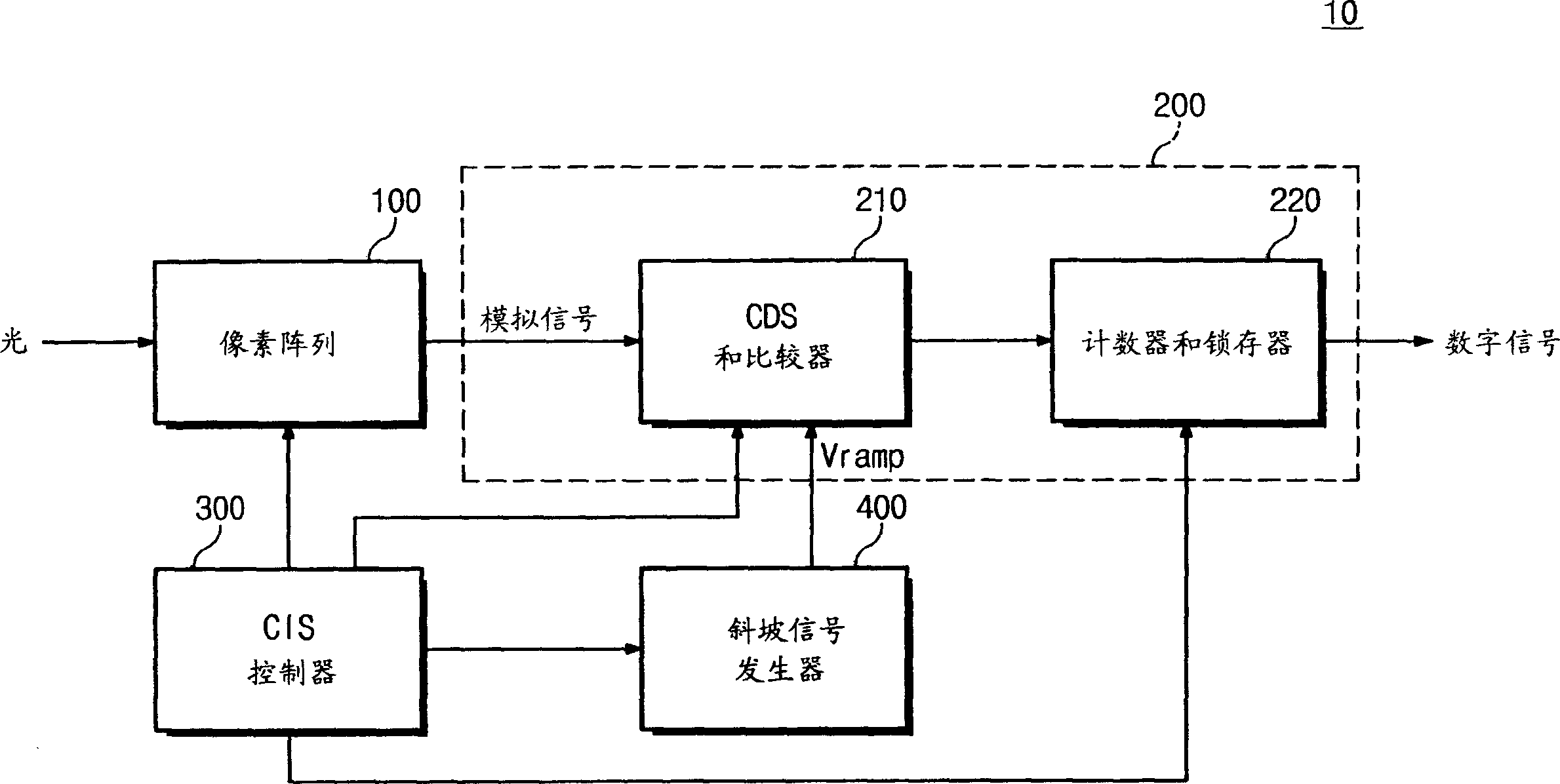
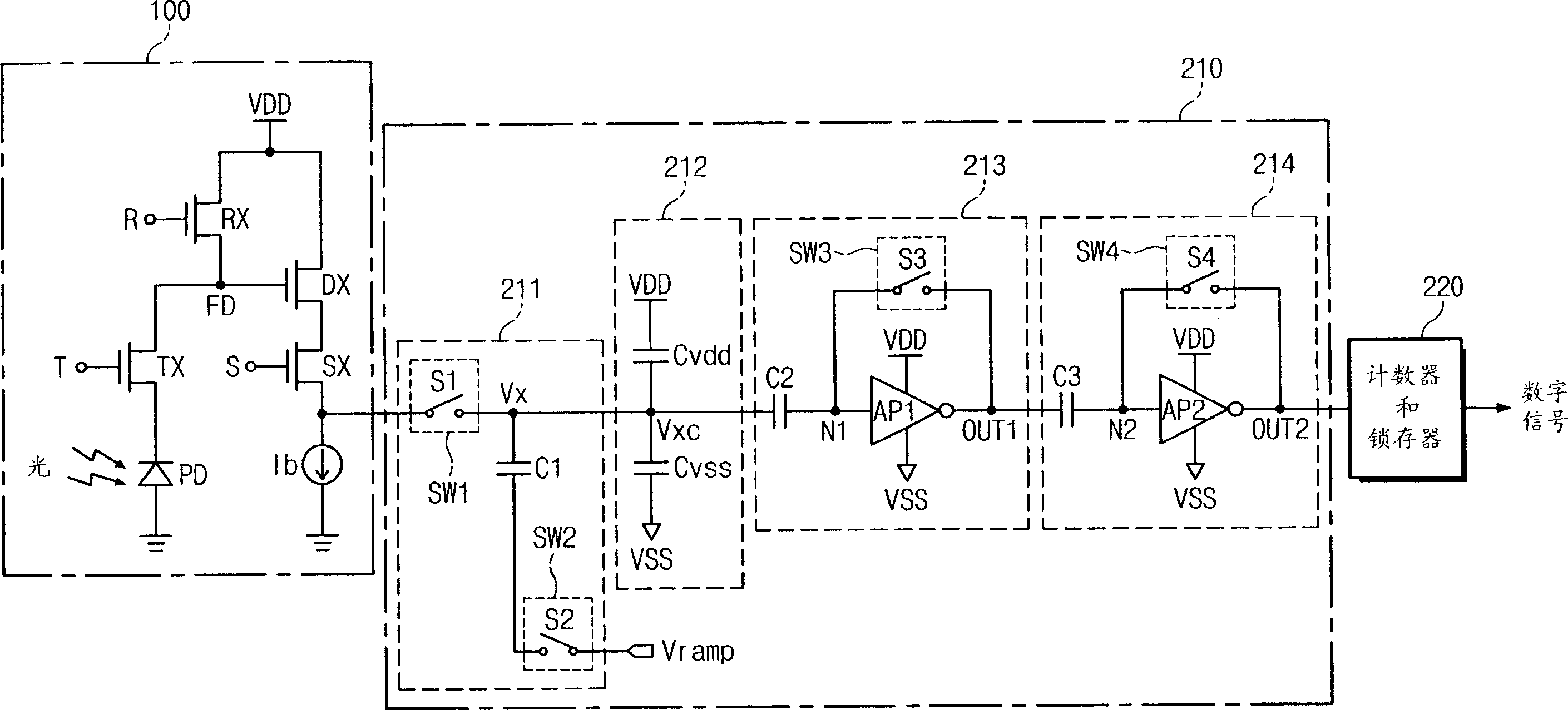
[0023] figure 1 is a block diagram of a CMOS (Complementary Metal Oxide Semiconductor) image sensor 10 according to an embodiment of the present invention. A CMOS image sensor (CIS) 10 includes a pixel array 100 , a correlated double precision sampling (CDS) ADC (Analog-Digital Converter) 200 , a CIS controller 300 and a ramp signal generator 400 .

[0024] The pixel array 100 is composed of a plurality of unit pixel circuits that generate electrical signals according to images. Each unit pixel circuit includes a photodiode for converting incident light of such an image into an analog image signal and for outputting such an image signal. The CDS ADC 200 includes a CDS (Correlated Double Precision Sampling) and comparator unit 210 and a conversion unit 220, which is implemented with a counter and a latch in one embodiment of the present invention. The CDS ADC 200 also includes a CIS controller 300 and a ramp signal generator 400 .

[0025] The CIS controller 300 generates co...


PUM


Abstract

An analog-to-digital converter includes an amplifying unit and a noise compensation unit. The amplifying unit amplifies a difference between a trip point voltage and a modified signal voltage. The trip point voltage has a first power noise component, and the noise compensation unit incorporates a second power noise component into an original signal voltage to generate the modified signal voltage. Thus, the power noise components are cancelled in the difference.

Description

technical field [0001] The present invention relates generally to an analog-to-digital converter in a CMOS (complementary metal-oxide-semiconductor) image sensor, and more particularly to compensation for power noise during such analog-to-digital conversion. Background technique [0002] Image sensors convert images into electrical signals using photo-conversion. Image sensors are generally classified as a Charge Coupled Device (CCD) type or a Complementary Metal Oxide Semiconductor (CMOS) Image Sensor (CIS) type according to a mechanism for generating and transferring charge carriers. [0003] The CCD image sensor transfers electrons generated by incident light to an output port using a gate pulse, and then converts the transferred electrons into a voltage. CCD image sensors have relatively high light sensitivity and reduced noise because the photocurrent is extracted after an accumulation time. However, CCD image sensors disadvantageously have a complicated driving mecha...

Claims


Application Information

Patent Timeline
Patent Type & Authority Applications(China)
IPC IPC(8): H03M1/08H03M1/12
CPCH03M1/0845H03M1/56H04N5/3575H04N5/378H04N25/616H04N25/75H04N25/60H04N25/77
Inventor 李明洙
Owner SAMSUNG ELECTRONICS CO LTD
Why Eureka
Try Eureka