Antenna structure on IC and manufacturing method

An on-chip antenna and integrated circuit technology, which is applied to the structural form of the radiation unit, the circuit, the antenna, etc., can solve the problems of increased energy loss of integrated antennas, increased overall length, and increased series resistance Rs of metal conductors, etc., to achieve reduction Energy loss, the effect of small energy loss

Inactive Publication Date: 2007-02-21
SHANGHAI INTEGRATED CIRCUIT RES & DEV CENT
View PDF3 Cites 26 Cited by
  • Summary
  • Abstract
  • Description
  • Claims
  • Application Information

AI Technical Summary

Problems solved by technology

The smaller the spacing, the stronger the magnetic field interaction, which will lead to more uneven current density in the metal conductor, making the series resistance Rs of the metal conductor larger, thereby affecting the increase in the energy loss of the integrated antenna on the chip; In the case of constant parameter

Method used


Image

  • Antenna structure on IC and manufacturing method
  • Antenna structure on IC and manufacturing method
  • Antenna structure on IC and manufacturing method

Examples


Embodiment Construction

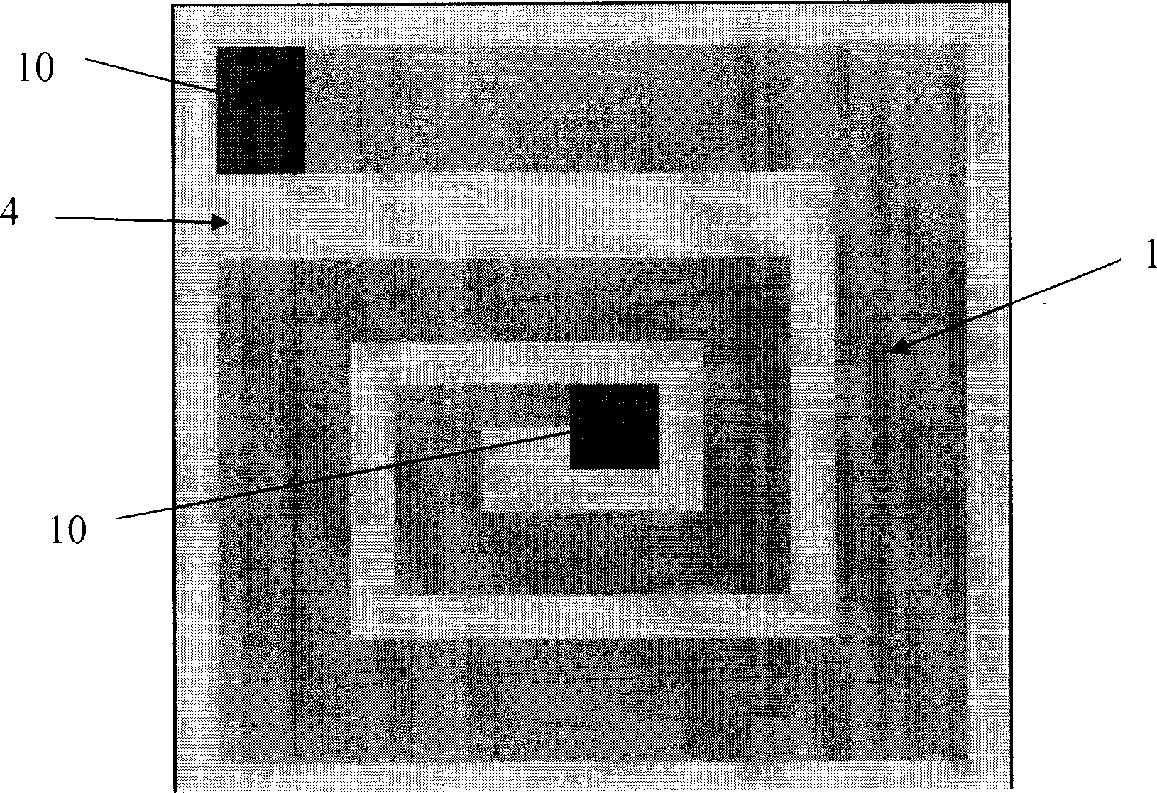
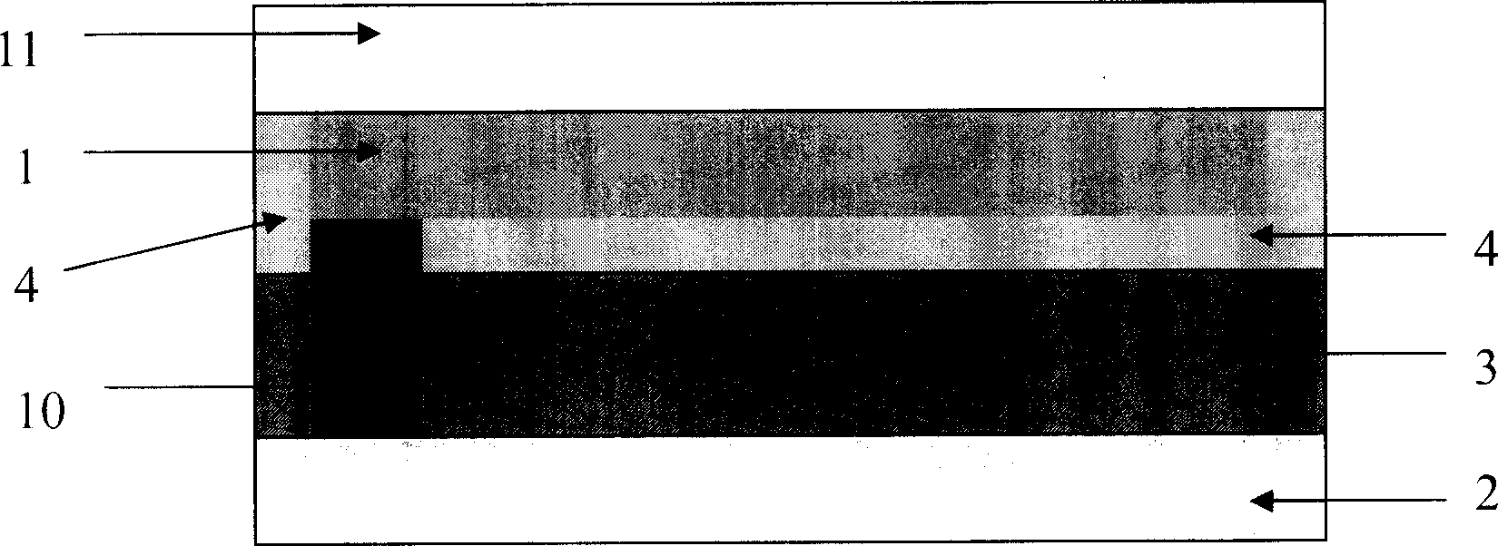
[0039] Please also refer to figure 1 , figure 2 with image 3 , an on-chip antenna structure in an integrated circuit of the present invention, after the integrated circuit chip 2 is manufactured, a first insulating material layer 3 and a second insulating material layer 4 are sequentially deposited on the chip surface, and on the second insulating material layer 4 The on-chip antenna 1 is manufactured in the present invention, the antenna 1 is connected to the bottom chip through the chip connection area 10, the periphery and the bottom of the antenna 1 are surrounded by the second insulating material layer 4, and a protective layer 11 of insulating material is deposited on the top of the antenna 1.

[0040] Wherein, the manufactured integrated circuit chip 2 includes all active and passive components and wiring.

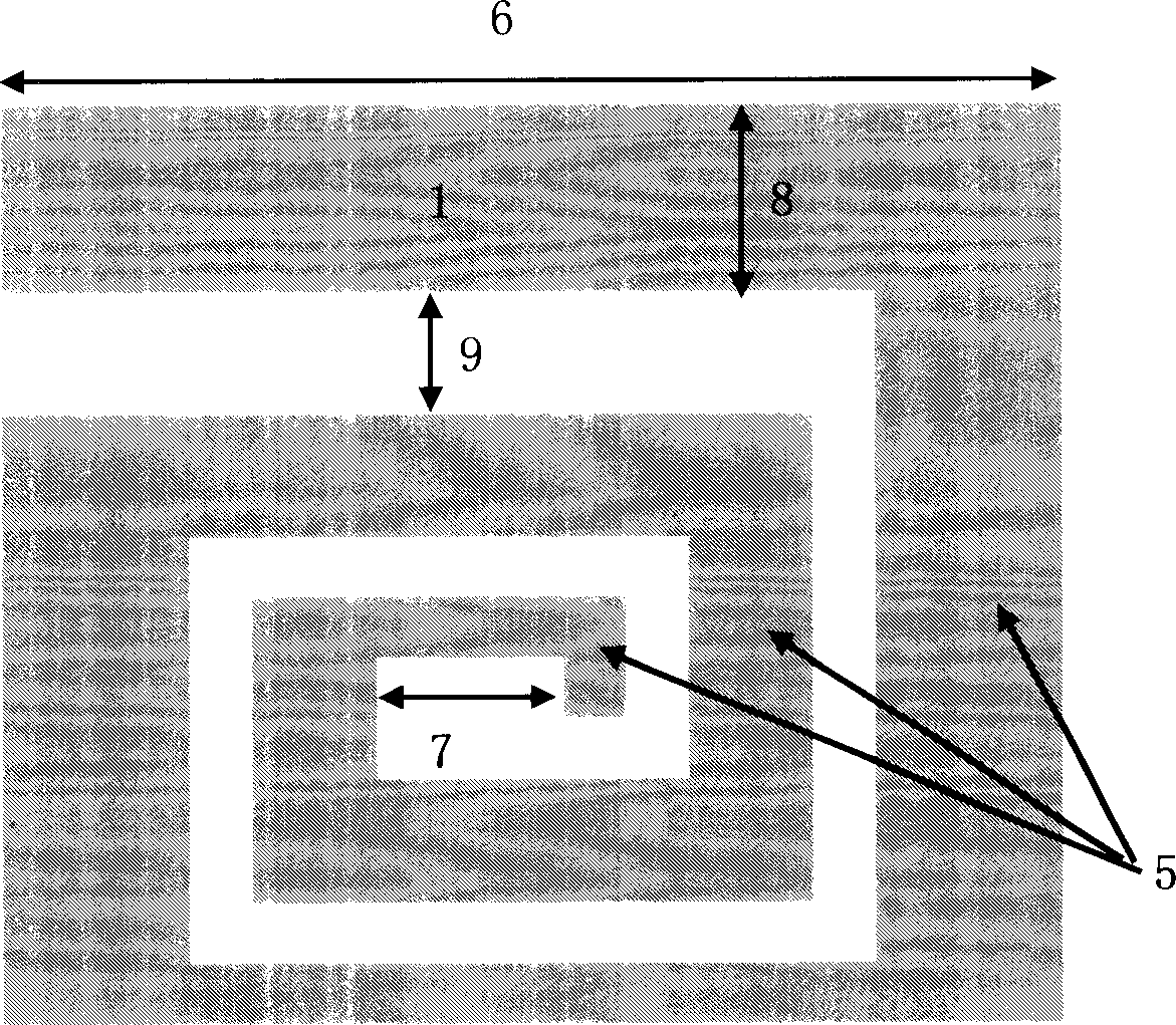
[0041] The antenna structure 1 of the present invention can be manufactured on the front side of the integrated circuit chip, can also be manufactured on the ba...


PUM

PropertyMeasurementUnit
Thicknessaaaaaaaaaa
Line widthaaaaaaaaaa

Abstract

Under precondition without changing size of external diameter, the invention discloses integrated antenna on chip. The helix structural antenna possesses gradual changed widths of metal coils and spans of metal coils in order to reduce serial equivalent resistance of helix coils so as to reduce energy loss. Comparing with traditional antenna on chip, the disclosed antenna on chip possesses features of lowering influence of eddy current effect and approach effect in high frequency so as to reduce the said equivalent resistance Rs, and energy loss. The preparing technique is compatible to conventional CMOS technique.

Description

technical field [0001] The invention belongs to the technical field of integrated circuit manufacturing, and in particular relates to a structure and a realization method of an on-chip integrated antenna of an integrated circuit chip. This patent is applicable to deep submicron / micron integrated circuit technology. Background technique [0002] Antenna is an indispensable part of wireless communication, and its basic function is to radiate and receive radio waves. When transmitting, the high-frequency current is converted into electromagnetic waves; when receiving, the electromagnetic waves are converted into high-frequency currents. As a key component in the radio frequency circuit, the antenna is the most difficult component to design and master in the circuit, and its performance parameters directly affect the performance of the radio frequency circuit. [0003] In the development of CMOS radio frequency integrated circuits (RFICs), the most urgent and difficult thing is...

Claims


Application Information

Patent Timeline
IPC IPC(8): H01Q1/38H01Q1/40H01Q7/00H01L21/77
Inventor 赵宇航
Owner SHANGHAI INTEGRATED CIRCUIT RES & DEV CENT
Why Eureka
Try Eureka