

Semiconductor chip assembly with metal containment wall and solder terminal
A technology of chip packaging structure and conductor chip, which is used in semiconductor devices, semiconductor/solid-state device parts, electric solid-state devices, etc.
- Summary
- Abstract
- Description
- Claims
- Application Information
AI Technical Summary
Problems solved by technology
Method used
Image

Examples
Embodiment Construction
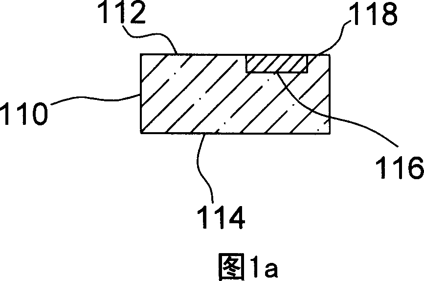
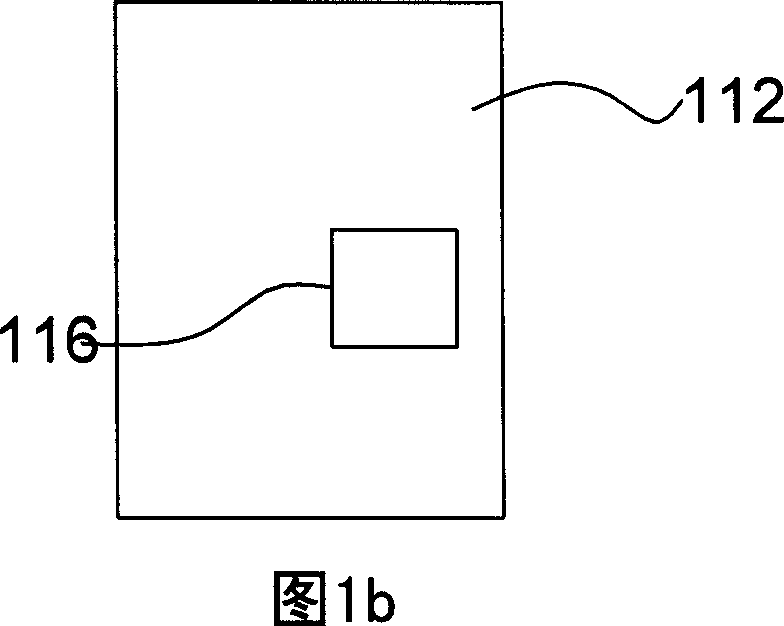
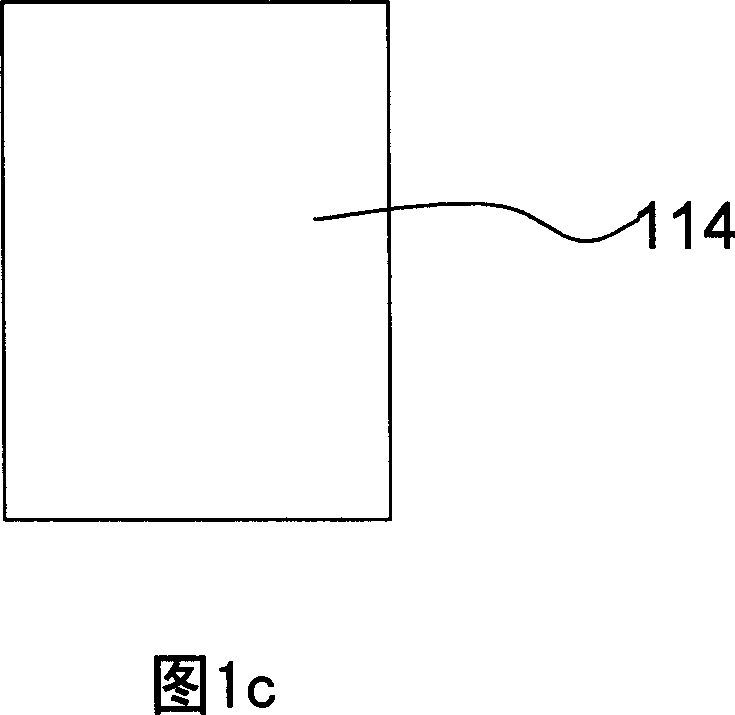
[0347] 1a to 27c are the first embodiment of the method for manufacturing a semiconductor chip package structure, wherein FIGS. 1a to 27a are schematic cross-sectional views, FIGS. 1b to 27b are schematic top views, and FIGS. 1c to 27c are schematic bottom views.
[0348] As shown in FIG. 1a, FIG. 1b and FIG. 1c, it is a schematic cross-sectional view of the semiconductor chip structure of the present invention, a schematic top view of the semiconductor chip structure of the present invention, and a schematic bottom view of the semiconductor chip structure of the present invention. As shown in the figure: the present invention is a semiconductor chip packaging structure with a metal wall at the welding end, wherein the semiconductor chip 110 is an integrated circuit, and is composed of a plurality of transistors, circuits, connecting parts and other connections (in the figure not shown). The semiconductor chip 110 includes a corresponding first plane 112 and a second plane 114...
PUM
 Abstract
Description
Claims
Application Information