Light-emitting device

A technology of light-emitting devices and light-emitting elements, which is applied in the direction of light-emitting materials, lighting devices, fluorescence, etc., can solve the problems of unusable and difficult to obtain products with low correlated color temperature, and achieve the effect of small deviation of black track

Active Publication Date: 2007-03-07
SHARP KK
View PDF4 Cites 7 Cited by
  • Summary
  • Abstract
  • Description
  • Claims
  • Application Information

AI Technical Summary

Problems solved by technology

In this Japanese Patent Laid-Open No. 2005-109085, there is no change at all compared with the previous white light-emitting device, and it is difficult to obtain a product with a low correlated color temperature.
[0014] On the other hand, a light-emitting element (peak wavelength: around 450nm) that emits blue light and (Y, Gd) activated by trivalent cerium that e...

Method used


Image

  • Light-emitting device
  • Light-emitting device
  • Light-emitting device

Examples


Embodiment 1

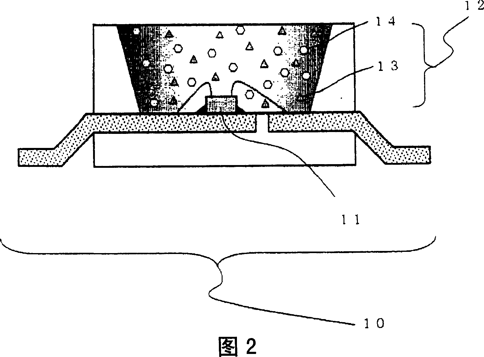
[0092] Fig. 2 is a schematic longitudinal sectional view of a light emitting device according to Embodiment 1 of the present invention. This light emitting device 10 includes: a light emitting element 11 that emits primary light; and a wavelength conversion unit 12 that absorbs at least part of the primary light and emits secondary light having a wavelength equal to or greater than the primary light wavelength. The wavelength conversion unit 12 includes a red light emitting phosphor 13 and a green light emitting phosphor 14 dispersed in a resin.

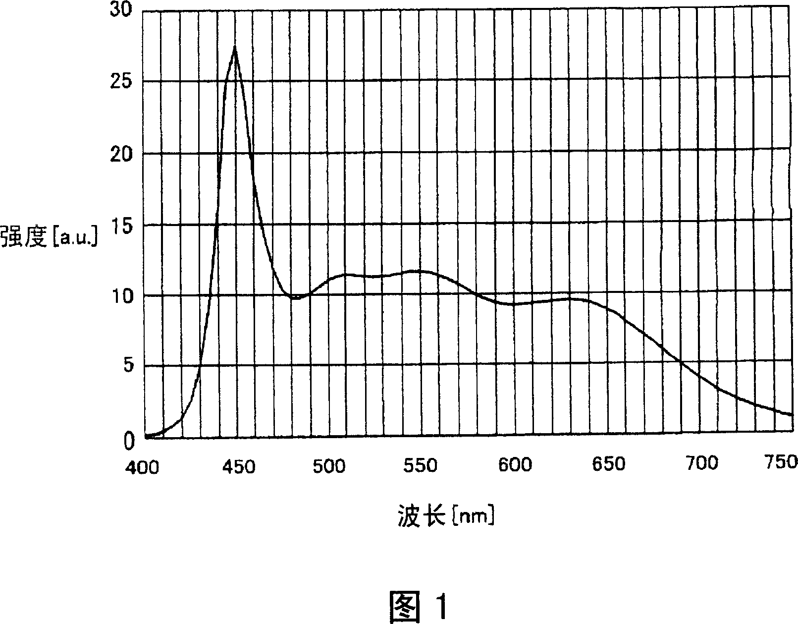
[0093] In Example 1, a gallium nitride (GaN)-based semiconductor having a peak wavelength of 450 nm was used as a light-emitting element. Ca used as a green light-emitting phosphor is included in the wavelength conversion part 3 (Sc 0.85 Ce 0.15 ) 2 (SiO 4 ) 3 (Particle size: 8.9μm), (Ca 0.98 Eu 0.02 )AlSiN 3 (Particle size: 3.8 μm). These green-based light-emitting phosphors and red-based light-emitting phosphors were mixe...

Embodiment 2

[0097] As a light-emitting element, a gallium nitride (GaN)-based semiconductor having a peak wavelength of 435 nm was used. In the wavelength conversion part, 9.3 μm 2 (Ba 0.60 Sr 0.38 Eu 0.02 )O·SiO 2 , and 50% by weight of 10.5 μm 2 (Sr 0.80 Ba 0.18 Eu 0.02 )O·SiO 2 , as a red light-emitting phosphor, a 3.6μm-containing (Ca 0.94 Mg 0.05 Eu 0.01 )(Al 0.99 In 0.01 )SiN 3 As a material, a mixture of these green-based light-emitting phosphors and a red-based light-emitting phosphor are mixed at a weight ratio of 1:0.31, dispersed in epoxy resin, and molded to form a wavelength conversion part. In this way, the light-emitting device in Example 2 having the structure shown in FIG. 2 was produced.

Embodiment 3

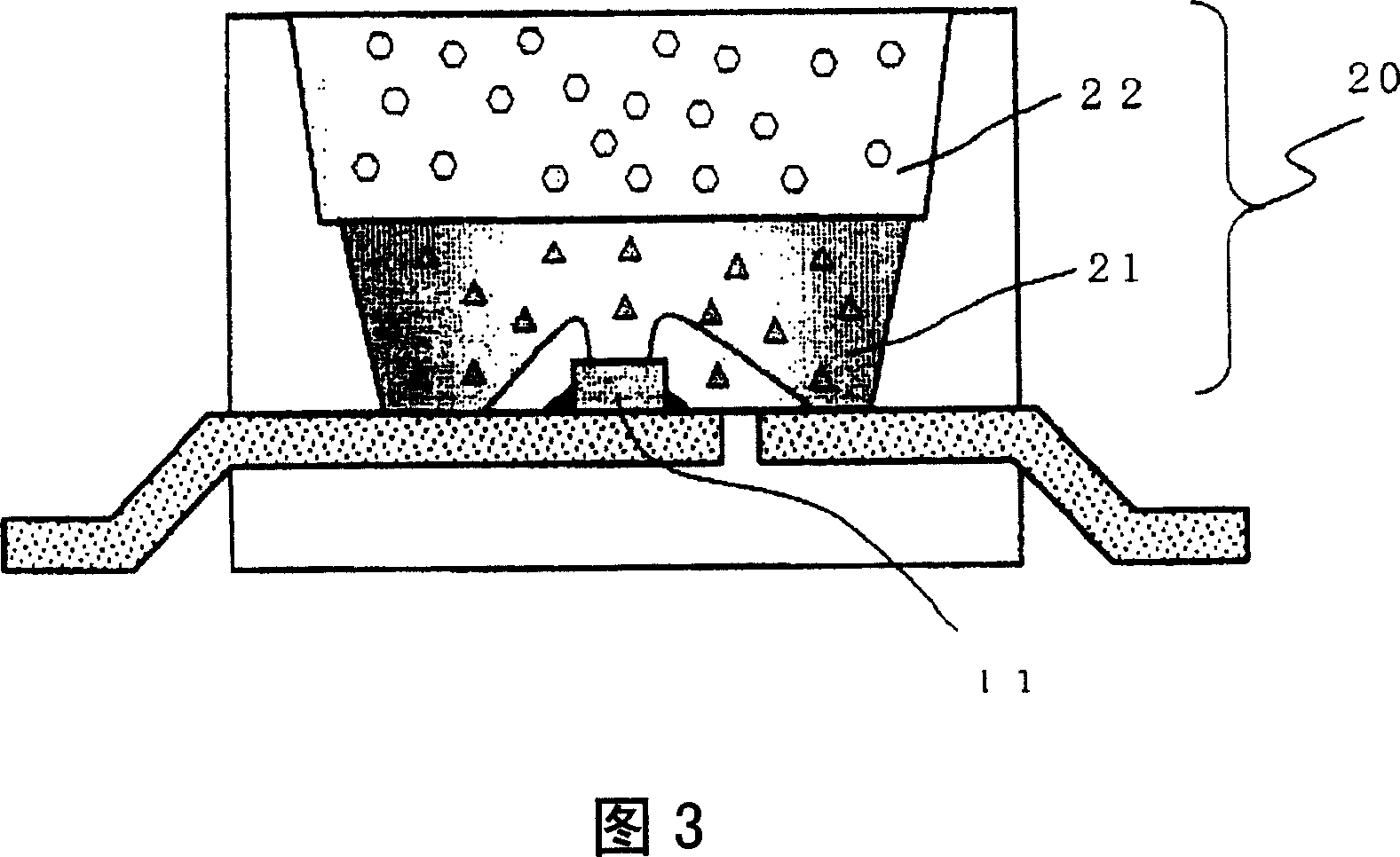
[0101] Fig. 3 is a schematic longitudinal sectional view of a light emitting device according to Embodiment 3 of the present invention. This light-emitting device includes: a light-emitting element 11 that emits primary light; and a wavelength conversion unit 20 that absorbs at least part of the primary light and emits secondary light having a wavelength equal to or greater than the primary light wavelength. The wavelength conversion unit 20 includes a resin layer (red light emitting phosphor layer) 21 containing dispersed red light emitting phosphors and a resin layer (green light emitting phosphor layer) 22 containing dispersed green light emitting phosphors. . Further, the red-based light-emitting phosphor layer 21 is disposed adjacent to the light-emitting element 11 , and the green-based light-emitting phosphor layer 22 is laminated thereon.

[0102] In Example 3, a gallium nitride (GaN) semiconductor having a peak wavelength at 435 nm was used as a light emitting elemen...


PUM

PropertyMeasurementUnit
Particle sizeaaaaaaaaaa

Abstract

A light-emitting device includes a light-emitting element emitting primary light and a wavelength conversion portion absorbing a part of the primary light and emitting secondary light having a wavelength equal to or longer than the wavelength of the primary light. The wavelength conversion portion includes a plurality of green or yellow light-emitting phosphors and a plurality of red light-emitting phosphors. The green or yellow light-emitting phosphor is implemented by at least one selected from a specific europium (II)-activated silicate phosphor (A-1) and a specific cerium (III)-activated silicate phosphor (A-2). The red light-emitting phosphor is implemented by a specific europium (II)-activated nitride phosphor (B). The light-emitting device emitting white light at efficiency and color rendering property higher than in a conventional example can thus be provided.

Description

technical field [0001] The present invention relates to a high-efficiency, high-color-rendering light-emitting device, which includes a light-emitting element that emits primary light and a wavelength conversion unit that absorbs the primary light and emits secondary light. Background technique [0002] A light-emitting device that combines a light-emitting element that emits primary light and a wavelength conversion unit that absorbs primary light and emits secondary light is expected to be a new-age light-emitting device that achieves low power consumption, small size, high brightness, and wide-ranging color reproducibility. The device has attracted much attention, and its research and development work is very active. The commonly used primary light emitted from the light-emitting element is the range from long-wavelength ultraviolet to blue, that is, 380nm to 480nm. In addition, in the wavelength conversion part, various phosphors suitable for different purposes are used...

Claims


Application Information

Patent Timeline
IPC IPC(8): F21K2/00H01L33/00C09K11/08F21K9/23F21K9/235F21Y113/13F21Y115/10
CPCY02B20/181
Inventor 增田昌嗣加藤正明猪口和彦梅田浩目见田裕一大内田敬藤田祐介尾本雅俊
Owner SHARP KK
Why Eureka
Try Eureka