

Method and system for loading FPGA target program
A target program and programming logic technology, applied in the field of data communication, can solve problems such as inability to upgrade online and long loading time, and achieve the effect of convenient maintenance and saving startup time
- Summary
- Abstract
- Description
- Claims
- Application Information
AI Technical Summary
Problems solved by technology
Method used
Image

Examples
Embodiment 1
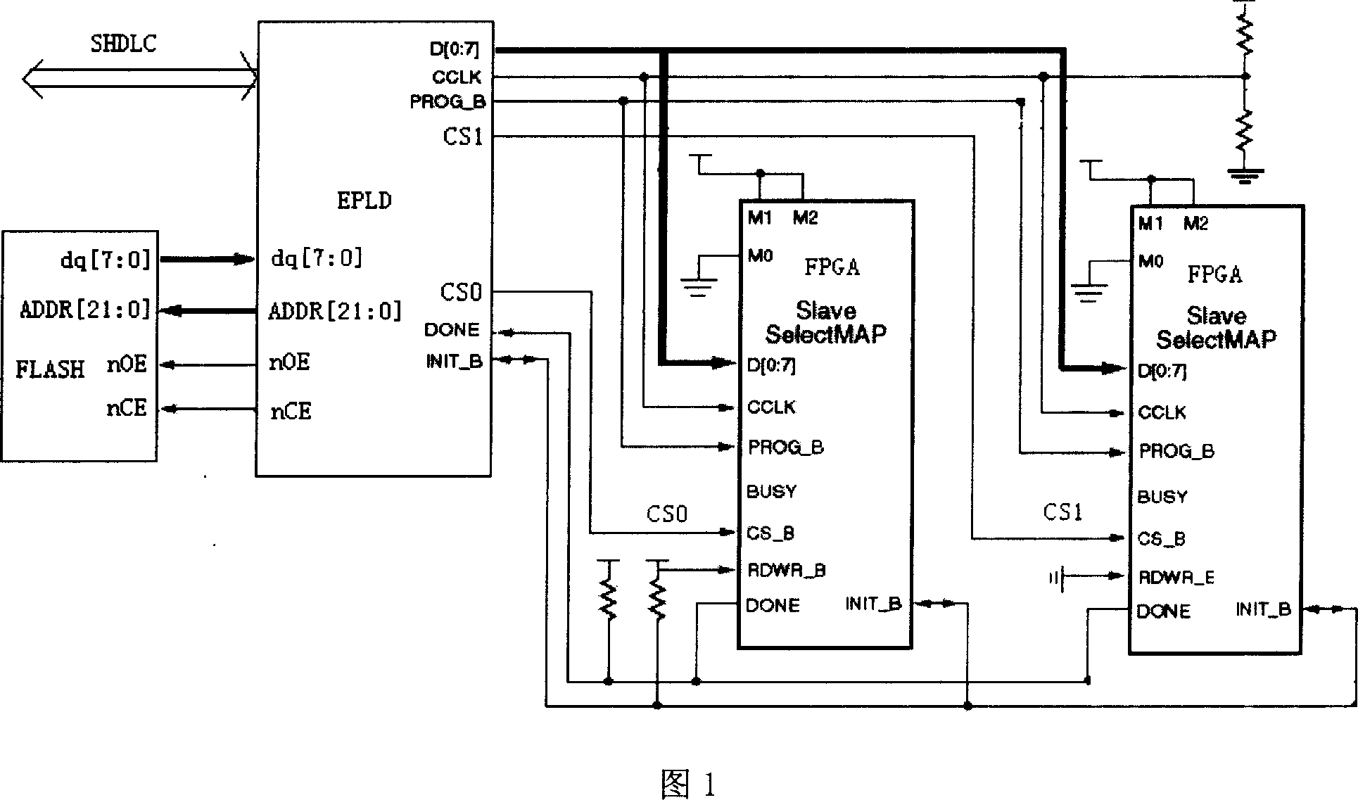
[0062]Referring to Figure 1, a piece of FLASH is plugged on the EPLD of the single board, and two FPGA chips are connected to the EPLD through the bus at the same time, and the two FPGA chips are connected in parallel. In this embodiment, there are two FPGA chips on the business processing single board to realize the large-scale business processing logic of the single board. It is required to realize fast loading of the two FPGA chips when the single board is powered on and to realize online upgrade of the system. .
[0063] Here we take the FPGA target program size as 2.11MB as an example to illustrate, then the single board design EPLD is plugged with a 4MB FLASH to store the FPGA target program. Since the logic functions of the two FPGAs on the single board are exactly the same, the EPLD adopts parallel and bus The way to load the FPGA.
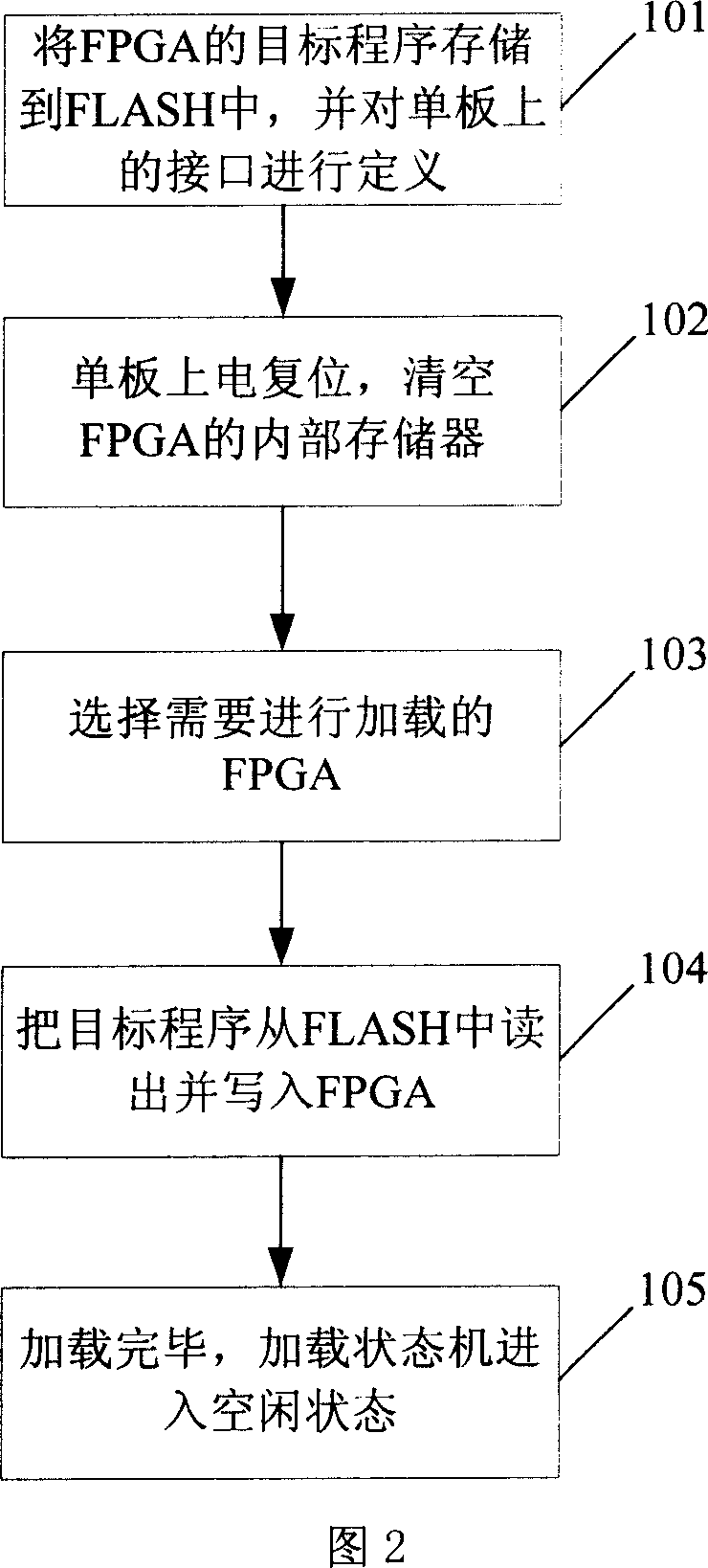
[0064] Referring to Fig. 2, the present invention provides a kind of method of loading FPGA target program, comprises the following step...
Embodiment 2
[0076] The main control board upgrades the target program in FLASH online through the interface of HDLC to Local Bus (local bus) and FLASH. After the online upgrade is completed, when the target program of the FPGA logic needs to be updated, the main control board sends a reload command, and the EPLD will start The FPGA loads the state machine to update and load the logic of the FPGA. If the target program of the FPGA logic does not need to be updated temporarily, reloading may not be performed.
[0077] The main control realizes online programming of FLASH through HDLC short frame paging, and EPLD realizes the conversion of HDLC to Local Bus and FLASH interface. Short-frame paging loading means that the capacity of each page is 128B. Divide the address of FLASH into three sections: Flash_addr[21:15], Flash_addr[14:7] and Flash_addr[6:0]. Set the HDLC writable register inside the EPLD. When HDLC performs a write operation on Flash, first write the FLASH The high address of t...
Embodiment 3
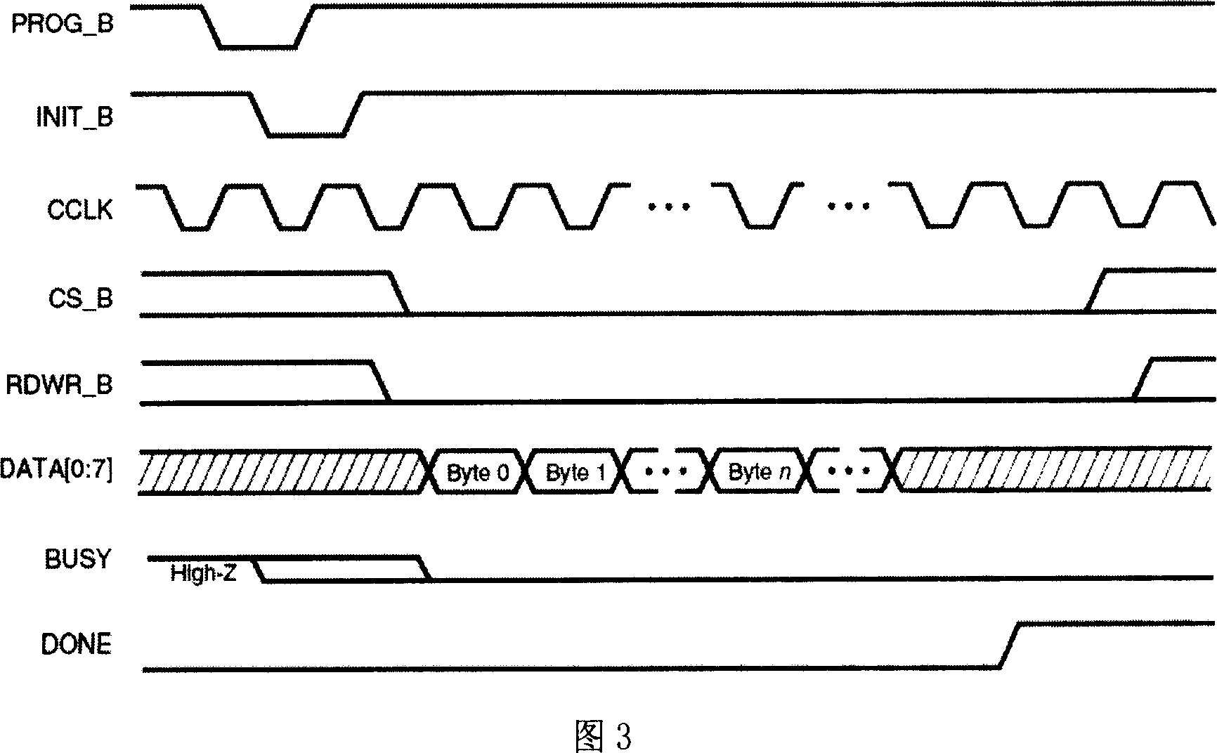
[0112] After the target program in FLASH is upgraded, when the FPGA target program needs to be updated, the main control board issues a reload command, and the EPLD will start the FPGA loading state machine, see Figure 6. The specific update and loading process includes the following steps:
[0113] Step 301: After the update of the target program in the FLASH is completed, the main control board sets the reload (heavy load) signal to "1", when the reload is set to "1", the EPLD logic enters the PROG_START state, and clears the reload in the PROGSTART state.
[0114] Steps 302 to 305 are the same as steps 102 to 105 to reload the FPGA, until the loading is complete and return to the IDLE state. I won't go into details here.
[0115] When two FPGAs are selected and loaded at the same time, the FPGA code is 2.11MB, the clock cycle is 1 / 6.25MHz=160ns, the time required for parallel input is 2.11MB×160ns, other states need about 5 cycles, and the FPGA STARTUP process takes about 5...
PUM
 Abstract
Description
Claims
Application Information