Pulse generating circuit, electronic device using this pulse generating circuit, and information transmitting method using this circuit

A technology for generating circuits and buffer circuits, applied in the direction of electric pulse generator circuits and logic circuits to generate pulses, etc., can solve the problems of increased energy consumption, impossibility, and difficulty in obtaining components, and achieve the effect of easy implementation

Inactive Publication Date: 2007-03-21
SEIKO EPSON CORP
View PDF2 Cites 9 Cited by
  • Summary
  • Abstract
  • Description
  • Claims
  • Application Information

AI Technical Summary

Problems solved by technology

[0012] However, to obtain the desired high frequency band pulses using the above-mentioned conventional pulse generation circuit, it is necessary to use components with sufficient speed, but in reality, it is very difficult or impossible to obtain such

Method used


Image

  • Pulse generating circuit, electronic device using this pulse generating circuit, and information transmitting method using this circuit
  • Pulse generating circuit, electronic device using this pulse generating circuit, and information transmitting method using this circuit
  • Pulse generating circuit, electronic device using this pulse generating circuit, and information transmitting method using this circuit

Examples


no. 1 Embodiment approach

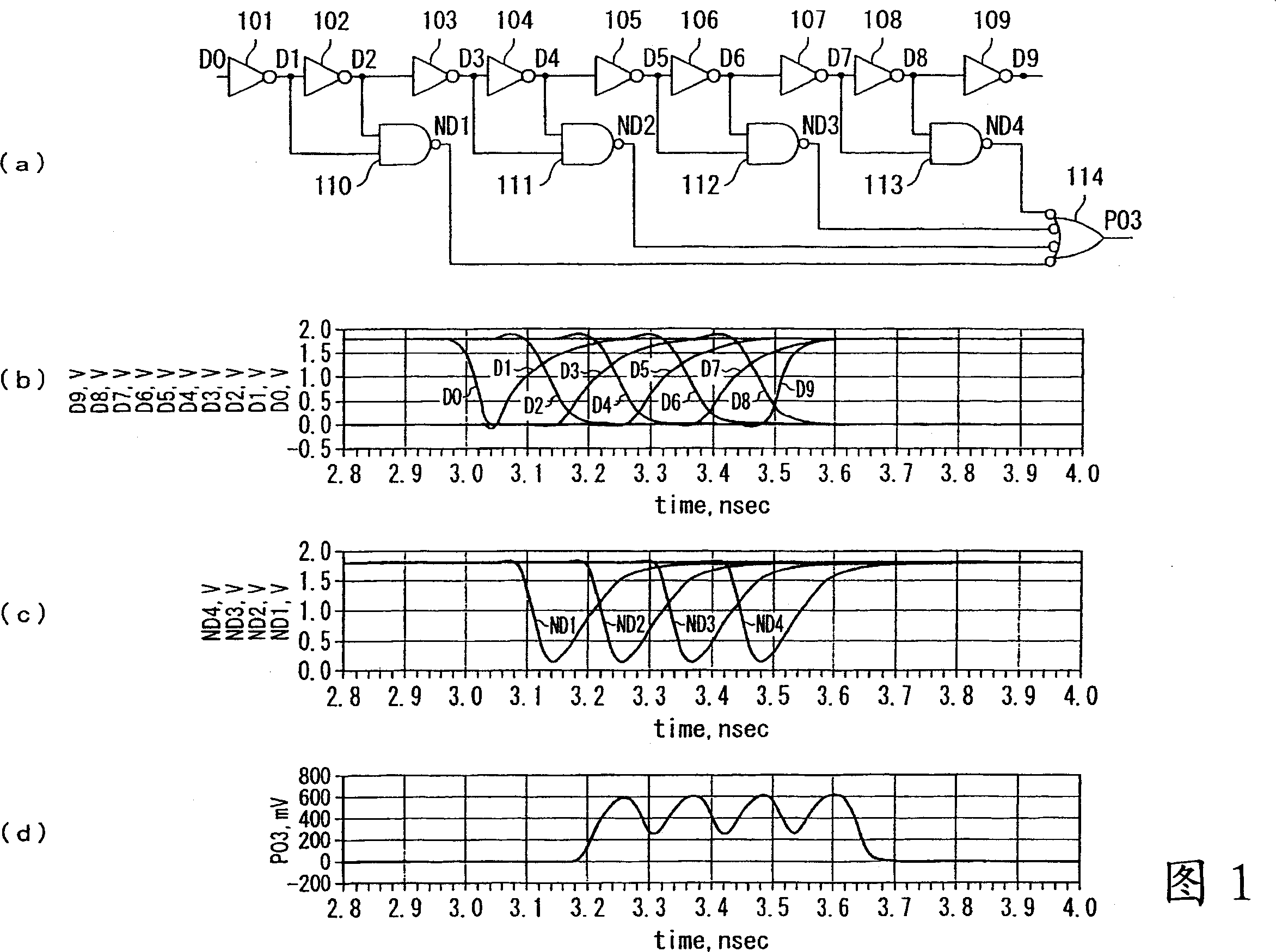
[0084] 1( a ) is a circuit diagram showing a main part of a pulse generating circuit according to the first embodiment of the present invention, and ( b ) to ( d ) are timing charts for explaining its operation. However, as an example, using the pulse waveform shown in Fig. 6(a) and using D Included in the case of four pulses (P D =8P W ) refers to pulses whose quantity is 4 for illustration.

[0085] Reference numerals 101 to 109 shown in FIG. 1( a ) denote inverter circuits connected in cascade. Each input / output terminal is given a terminal name like D0-D9.

[0086] When the input terminal D0 changes from a high level (H) to a low level (L) as shown in (b), each output propagates with a delay of t.

[0087] When both of D1 and D2, D3 and D4, D5 and D6, and D7 and D8 are H respectively, NAND circuits 110-113 output L from terminals ND1-ND4 as shown in (c). When one of ND1 to ND4 is L, the "NOR" (NOR) circuit (NOR circuit of negative logic) 114 outputs H as shown in figu...

no. 2 Embodiment approach

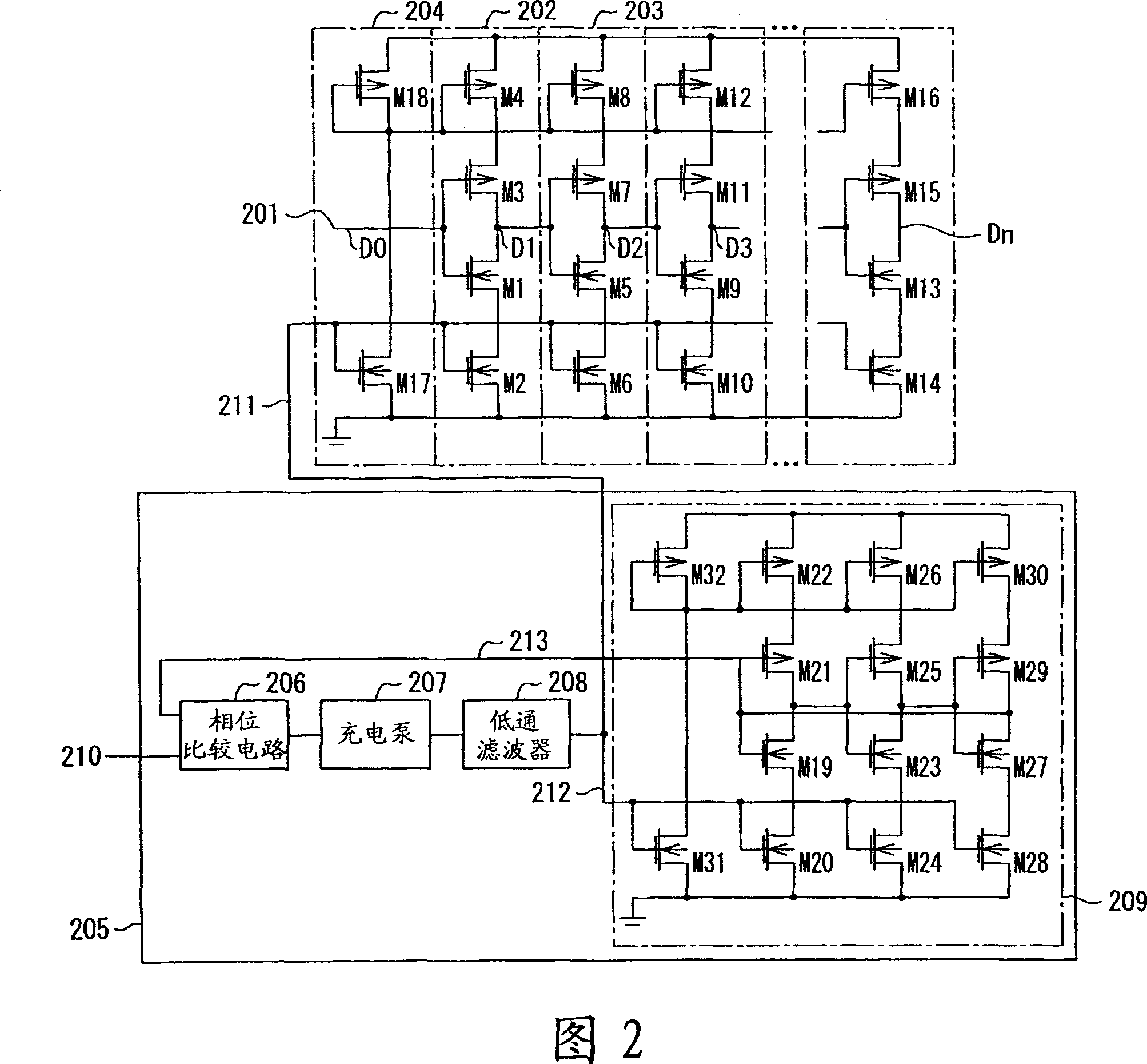
[0094] FIG. 2 is a circuit diagram showing main parts of a pulse generating circuit according to a second embodiment of the present invention.

[0095] Reference numerals 202 and 203 denote inverter circuits with a controllable delay amount, and correspond to the inverter circuits 101 and 102 constituting the delay circuit in the first embodiment. The same circuits are used by arranging them in desired stages. In Figure 2, levels 3 onwards are not numbered. This inverter circuit 202 is constituted by a combination of a PMOS transistor M3 and an NMOS transistor M1.

[0096] The PMOS and NMOS transistors M4 and M2 are connected to the sources of the respective transistors M3 and M1, and by using these M4 and M2 to control the amount of current flowing into the inverter circuit using M3 and M1, the amount of delay thereof can be controlled.

[0097] The gate of the transistor M2 is connected to the control voltage terminal 211, and the gate of the transistor M4 is connected to ...

no. 3 Embodiment approach

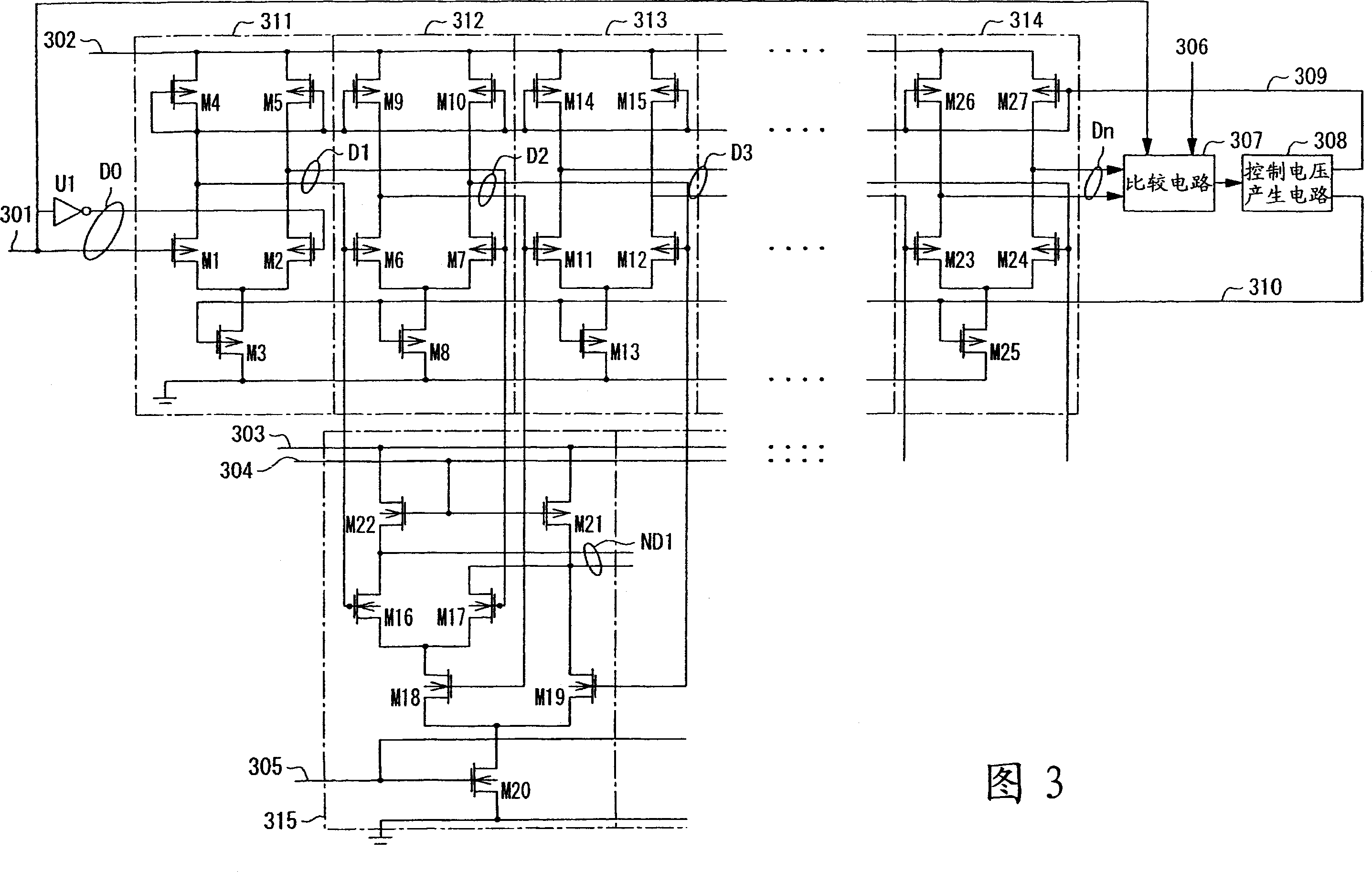
[0109] 3 is a circuit diagram showing main parts of a pulse generating circuit according to a third embodiment of the present invention.

[0110] 311 to 314 are buffer circuits composed of current mode logic circuits. Taking the buffer circuit 311 as an example to describe its interior, the differential amplifier circuit is composed of a differential pair of NMOS transistors M1 and M2. The NMOS transistor M3 limits the circuit current according to the control voltage 310 applied to its gate, thereby controlling the amount of delay. The PMOS transistors M4 and M5 are loads on the output side, and the output amplitude is controlled according to the voltage applied to their gates. The buffer circuit 311 is input and output driven by a differential signal which is a characteristic of a current mode logic circuit.

[0111] Furthermore, the terminal 301 is a trigger terminal and corresponds to the terminal D0 of the first embodiment, and a target pulse is generated based on a puls...


PUM


Abstract

The invention provides a pulse generating circuit, a device using the same and an information transmitting method. The pulse generating circuit can easily generates a high frequency band pulse with a low energy consumption by using a simple circuit without using a high-cost semiconductor process. The pulse generating circuit is composed of: inverter circuits (101-109) which are connected in series according to a predetermined amount of stage; a plurality of NAAD circuits (110-113) which are connected with the input/output side of one of the inverter circuits (101-109) every other one stage, generating a pulse with a width which is equal to a delay of each stage of the connected inverter circuits (102, 104, 106, 108); and a NOR circuit (114) which obtains an 'or' of the output of the NAND circuits (100-113).

Description

technical field [0001] The present invention relates to a pulse generation circuit suitable for UWB (Ultra Wide Band) communication, an electronic device using the circuit, and an information transmission method using the circuit. Background technique [0002] UWB communication is a communication method for high-speed and large-capacity data communication using a very wide frequency band. The communication methods using broadband signals include the traditional spread spectrum-based method and the Orthogonal Frequency Division Multiplexing (OFDM) method. However, UWB is an ultra-wideband communication method using very short pulses, also known as pulse radio (IR) ) way of communication. In the IR method, regardless of conventional modulation, modulation and demodulation can be performed simply by manipulating the time axis, and it is considered that simplification of circuits and reduction in power consumption can be expected (see Patent Documents 1, 2, and 3). [0003] He...

Claims


Application Information

Patent Timeline
IPC IPC(8): H03K3/02H03K3/027
Inventor 池田胜幸
Owner SEIKO EPSON CORP
Why Eureka
Try Eureka