Method and system for operating physical gas-phase deposition

A physical vapor deposition and device technology, which is applied in metal material coating process, ion implantation plating, coating, etc., can solve the problems that are difficult to realize, and achieve the effect of high device output

Inactive Publication Date: 2007-04-04
SEMICON MFG INT (SHANGHAI) CORP +1
View PDF0 Cites 0 Cited by
  • Summary
  • Abstract
  • Description
  • Claims
  • Application Information

AI Technical Summary

Problems solved by technology

As devices become smaller, sputtered films require higher uniformity, which is difficult to achieve with existing technologies

Method used


Image

  • Method and system for operating physical gas-phase deposition
  • Method and system for operating physical gas-phase deposition
  • Method and system for operating physical gas-phase deposition

Examples


Embodiment Construction

[0019] According to the present invention, there are provided techniques related to integrated circuits and integrated circuit processing methods for manufacturing semiconductor devices. More specifically, the present invention provides a method and system for operating a physical vapor deposition process using active feedback control for fabricating semiconductor integrated circuit devices. It should be recognized, however, that the invention has broader applicability. For example, the invention can be applied to various other applications such as displays, MEMS.

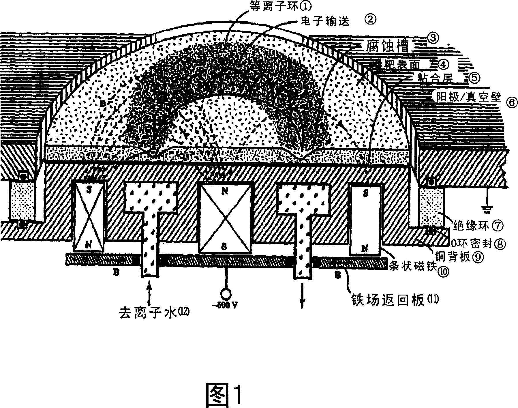
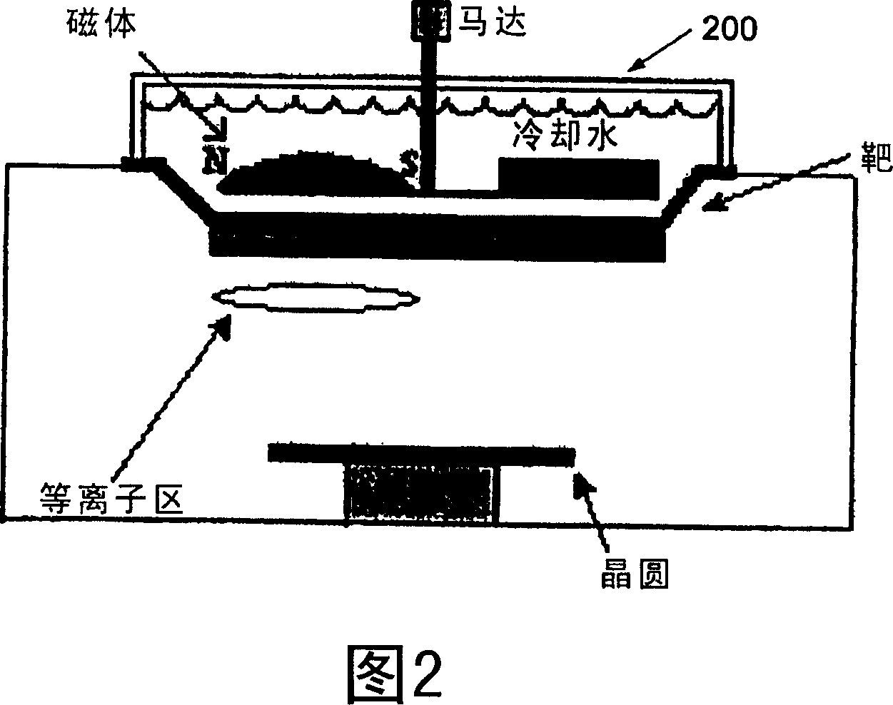
[0020] FIG. 1 is a simplified cross-sectional illustration of a conventional PVD system 100 . As shown, a PVD system (which is widely used to deposit metal layers and related materials in the process of fabricating semiconductor integrated circuits) includes a flat metal target to be sputtered and a wafer to be coated opposite the metal target. Working gas (usually argon) fills the reaction chamber at low pressur...


PUM


Abstract

This invention provides a kind of method that using the physics gas phase aggradation process semiconductor crystal round, including laying underlayment in the pedestal of the reaction room. The surface of the underlayment draws near the target material that in the reaction room. Target material includes the first face and second face which are set to the surface of the underlayment. The method includes operating the magnet component which is fixed around the revolution component, the revolution component is coupled with the reaction room and coupled with the driving motor and the driving motor is coupled to the drive. The magnet component is put in the place with destine dimension from the centre area of the revolution component. The method includes the magnet component which moves around the centre area by making use of the revolution component. The magnet component rotates with the speed v and affects the space covered in the second surface of the target. The method includes gaining information which relates to the magnet component, the electromagnetic field is relevant to the moving magnet component. The method includes handling information to ascertain if the electromagnetic field is in the preconcert parameter. It transmits the signal to drive to adjust magnet component speed and then to change the electromagnetic field.

Description

technical field [0001] The present invention relates generally to integrated circuits and integrated circuit processing methods for fabricating semiconductor devices. More specifically, the present invention provides a method and system for operating a physical vapor deposition process using active feedback control for fabricating semiconductor integrated circuit devices. It should be recognized, however, that the invention has broader applicability. For example, the invention can be applied to various other applications such as displays, MEMS. Background technique [0002] Over the past few decades, integrated circuits have grown from a handful of interconnected devices fabricated on a single silicon wafer to millions of devices. Current integrated circuits offer performance and complexity far beyond what was originally envisioned. In order to achieve progress in complexity and circuit density (i.e., the number of devices that can be packaged on a given chip area), the m...

Claims


Application Information

Patent Timeline
Patent Type & Authority Applications(China)
IPC IPC(8): C23C14/34C23C14/56
Inventor 温家琳
Owner SEMICON MFG INT (SHANGHAI) CORP
Why Eureka
Try Eureka