Sputtering coating method for high-shielding thin-film against electromagnetic interference on plastic matrix

An anti-electromagnetic interference, plastic substrate technology, applied in the direction of sputtering plating, ion implantation plating, vacuum evaporation plating, etc., can solve the problems of plastic deformation, shielding effect can not reach 70dB, low production efficiency, etc., to reduce Unit impedance, enhanced anti-electromagnetic interference effect, and improved production efficiency

Inactive Publication Date: 2007-04-04
MITAC PRECISION TECH CO LTD SHUNDE DISTRICT FOSHAN CITY
View PDF0 Cites 4 Cited by
  • Summary
  • Abstract
  • Description
  • Claims
  • Application Information

AI Technical Summary

Problems solved by technology

However, in order to avoid plastic deformation due to high temperature during sputtering, usually the sputtering temperature should not be set higher. Due to the temperature problem of sputtering, the thickness of one sputtering needs to be controlled within 0.7 μm. The shielding effect cannot reach 70dB. For example, a copper film with a thickness of about 0.5-0.7μm can only be plated at one time, and its shielding effect can only reach 57dB. Plastic products must leave the vacuum sputtering device to cool in the atmosphere before repeated sputtering, that is, It is said that it is necessary to repeatedly enter the vacuum sputtering device and leave the cooling for at least three times to achieve a copper film with a thickness of about 2 μm so that the shielding effect can reach more than 70dB. Affect equipment output, lower production efficiency

Method used


Image

  • Sputtering coating method for high-shielding thin-film against electromagnetic interference on plastic matrix
  • Sputtering coating method for high-shielding thin-film against electromagnetic interference on plastic matrix

Examples


Embodiment Construction

[0021] In order to further understand the features and technical contents of the present invention, please refer to the following detailed description and accompanying drawings of the present invention. However, the accompanying drawings are provided for reference and illustration only, and are not intended to limit the present invention.

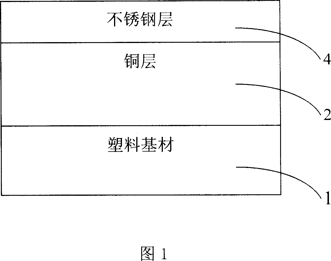
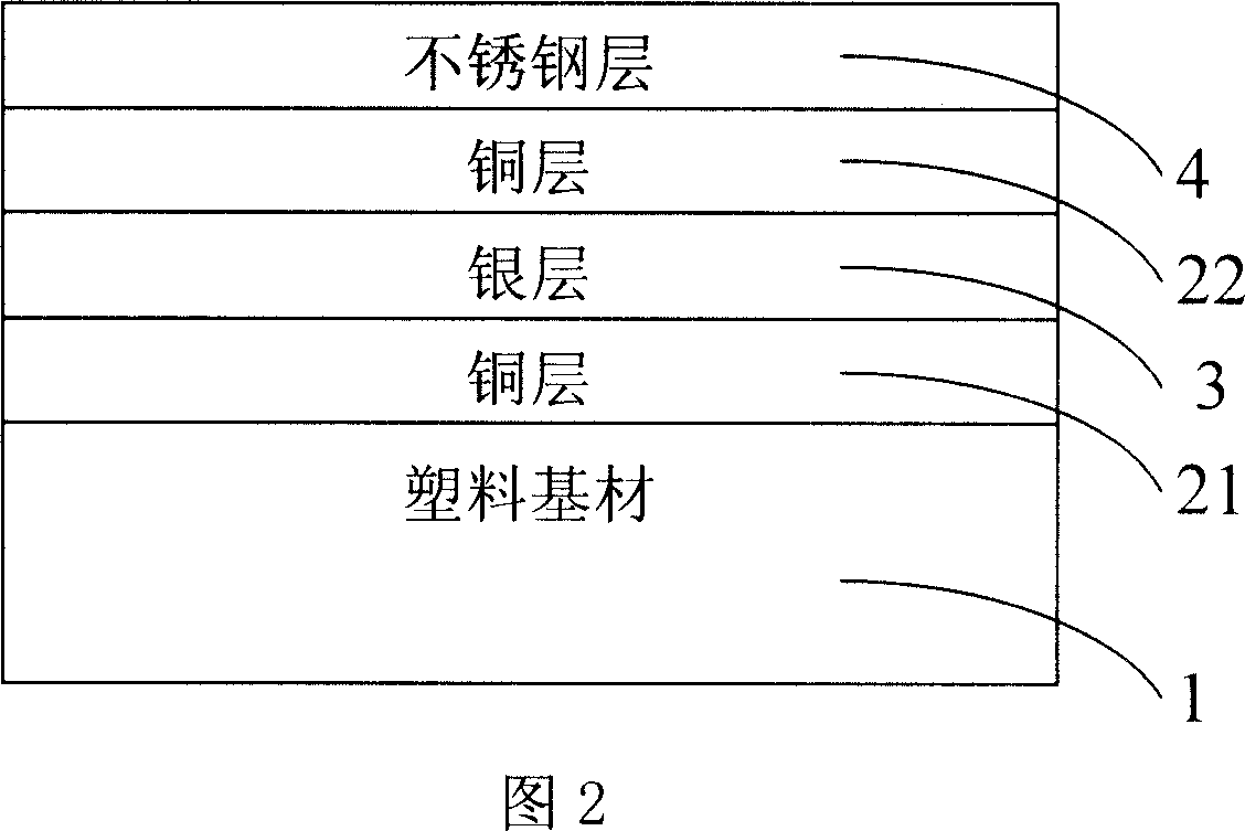
[0022] As shown in Figure 2, the sputtering method of plating high shielding anti-electromagnetic interference film on the plastic substrate of the present invention comprises the steps:

[0023] In the sandblasting treatment step, the surface of the plastic substrate 1 is sandblasted with brown corundum sand grains or white corundum sand grains;

[0024] In the cleaning step, the surface of the plastic substrate 1 that has been sandblasted is cleaned with ultrasonic waves, and the sand grains on the surface of the plastic substrate 1 are washed away;

[0025] In the film coating step, a layer of copper film 21 is plated on the surface of t...


PUM


Abstract

A kind of sputter method that plating high defilade guarding against electromagnetism disturbance film on the plastic base material, it includes the following steps: Sand blast handle step, gushing in the surface of base material by using the corundum grits; cleaning step, using ultrasonic wash the outside of the base material which has done the sand blast handles; plating step ,plating a layer of cupper film in the surface of the plastic base material with the vacuum sputter method, plating a layer of silver film again, then plating a layer of copper film again to compose of the sandwich plating tier structure that 'copper + silver + copper '. Using the sputtering method in this invention, 'copper + silver + copper ' sandwich plating tier structure is benefit to reducing a unit impedance of the film, strengthening the effect that defending against the interfere of the electromagnetism, it can also form the 'copper/ silver/ copper/ stainless steel ' plating structure at one time in a sputter, whose block effect can reach the efficacy that above 70 dB, it is benefit to improving the production effect.

Description

technical field [0001] The invention relates to a method for coating a film on the surface of a product, in particular to a physical coating method for coating a high shielding and anti-electromagnetic interference film on the surface of a plastic substrate by vacuum sputtering. Background technique [0002] Plating a characteristic and strong adhesion coating on the surface of the plastic substrate can achieve the purpose of protecting the substrate, decorating, anti-electromagnetic wave, conducting electricity or anti-reflection. Plating an electromagnetic interference (EMI, English full name for Electromagnetic Interference) protective film on the surface of the plastic substrate is one of the common and important implementations. The shielding effect of the μm copper film 2 can reach more than 70dB, and a layer of stainless steel film 4 is usually plated for surface anti-corrosion protection. [0003] The process of coating the surface of plastic parts has a long histor...

Claims


Application Information

Patent Timeline
Patent Type & Authority Applications(China)
IPC IPC(8): C23C14/34C23C14/02G12B17/02
Inventor 吴政道
Owner MITAC PRECISION TECH CO LTD SHUNDE DISTRICT FOSHAN CITY
Why Eureka
Try Eureka