TFT LCD array substrate structure and method for forming non-comformal insulation film and use

An array substrate structure and insulating thin film technology, applied in nonlinear optics, instruments, semiconductor devices, etc., can solve the problems of thin film transistor device failure, liquid crystal display device dead pixels, etc., to reduce invisible defects and display dead pixels, reduce Development costs and usage costs, effects of relaxed dependencies

Active Publication Date: 2007-04-11
K TRONICS (SUZHOU) TECH CO LTD +1
View PDF1 Cites 9 Cited by
  • Summary
  • Abstract
  • Description
  • Claims
  • Application Information

AI Technical Summary

Problems solved by technology

Such invisible defects cause failure of thin film transistor devices and dead pixels of liquid crystal display devices

Method used


Image

  • TFT LCD array substrate structure and method for forming non-comformal insulation film and use
  • TFT LCD array substrate structure and method for forming non-comformal insulation film and use
  • TFT LCD array substrate structure and method for forming non-comformal insulation film and use

Examples


Embodiment 1

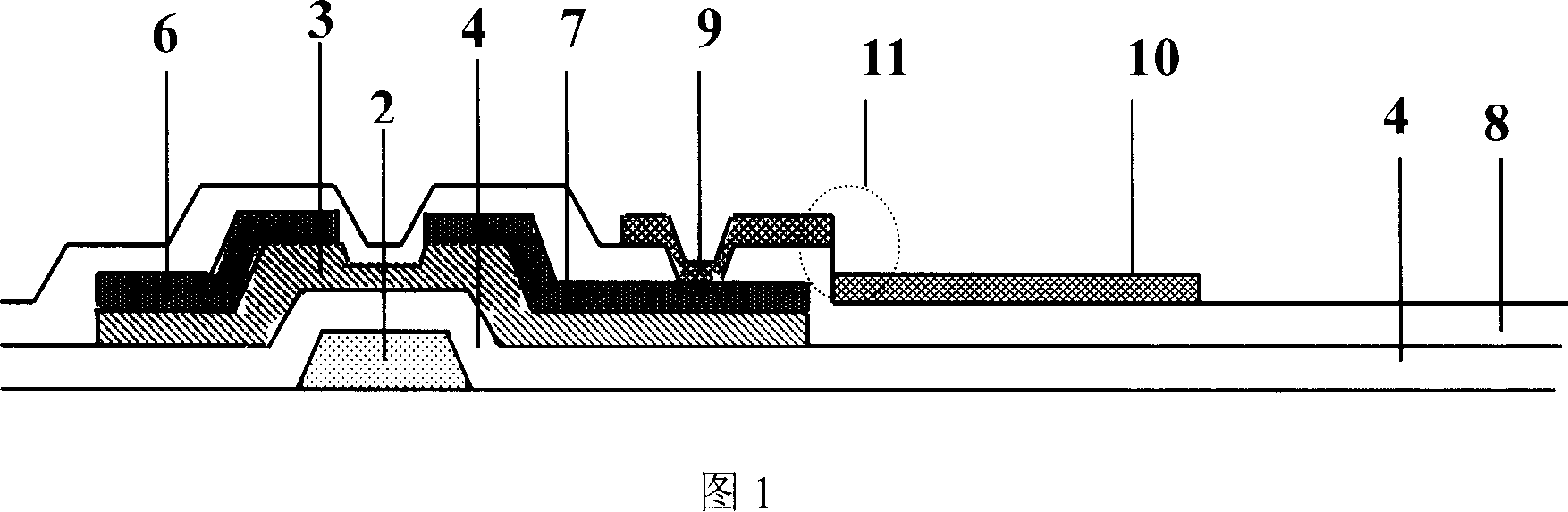
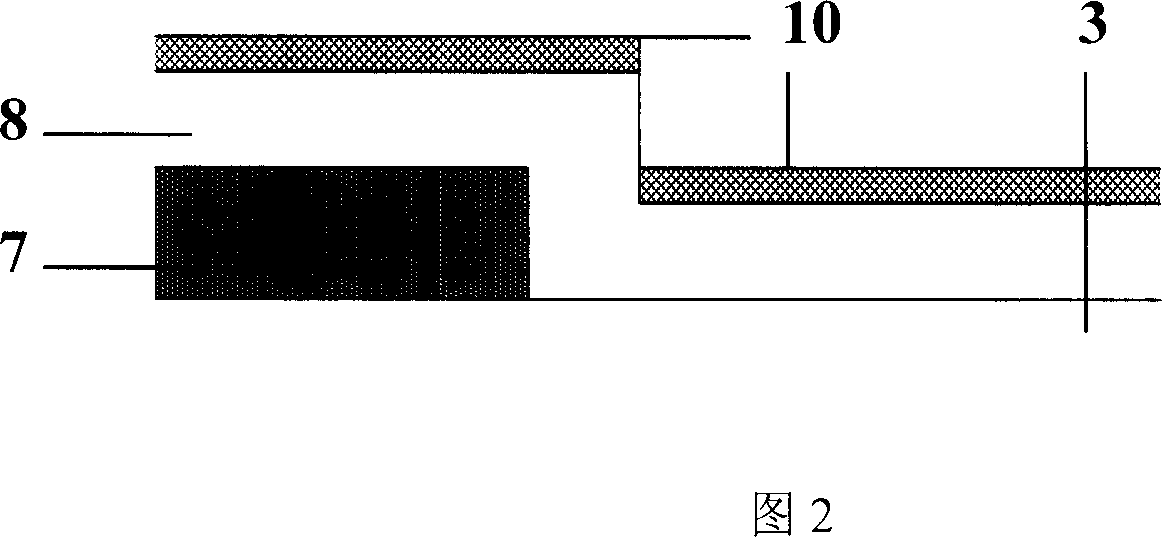
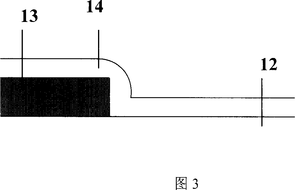
[0047] First, as shown in FIG. 3 , a substrate 12 on which a conductive film 13 (which may be a gate electrode film or a source-drain electrode film, etc.) has been formed is provided.

[0048] Then, the aforementioned substrate 12 is placed in the plasma-enhanced chemical vapor deposition equipment. In addition to passing reactive gases such as silane, ammonia and nitrogen to the plasma-enhanced chemical vapor deposition equipment for depositing insulating films, the inert gases such as argon, Or helium, or a mixed gas of helium and hydrogen, the film is etched while the film is deposited to form a non-conformal insulating film 14 . For example, the inert gas argon is fed into the plasma, and the generated argon ions are accelerated to the surface of the substrate under the action of an electric field, and bombard the surface film, resulting in film etching while depositing the film. As shown in FIG. 3 , the insulating film 14 above the conductive film 13 forms a non-conforma...

Embodiment 2

[0050] Figures 4a to 4d show the specific fabrication process of this embodiment.

[0051] Firstly, a substrate 12 on which a conductive thin film 13 (may be a gate line and a gate electrode or a source-drain electrode, etc.) has been formed is provided.

[0052] Subsequently, the substrate 12 is placed in the plasma-enhanced chemical vapor deposition equipment, and reactive gases such as silane, ammonia, and nitrogen are introduced into the reaction chamber. After a certain period of time, a first layer of insulating film 14a with a certain thickness is deposited to stop the reaction. Gas access. Due to the inherent conformal properties of plasma enhanced chemical vapor deposition, the first insulating film 14a forms vertical steps as shown in FIG. 4a.

[0053] Next, the inert gas is fed into the plasma-enhanced chemical vapor deposition equipment, and the inert gas plasma is generated under a certain power and pressure, and the inert gas ions bombard the surface of the subs...


PUM

PropertyMeasurementUnit
thicknessaaaaaaaaaa

Abstract

This invention discloses a TFT LCD array base plate structure including: a base plate, grid lines, a grid electrode, a grid insulation film, an active layer isolated island, a data line, a source, a drain, a transparent conduction film and a passivation insulation film, in which, the grid insulation film is a non-conformal structure or the passivation insulation film is a non-conformal structure or both of them are the non-conformal structure. This invention discloses a forming method for two non-conformal structures and the TFT LCD array base plate structure.

Description

technical field [0001] The invention relates to a TFT LCD array substrate structure and a manufacturing method thereof, in particular to a TFT LCD array substrate structure in which the insulating film is non-conformal, and a method for forming the non-conformal insulating film and its application. Background technique [0002] In order to realize high-definition and large-capacity display, a display device generally uses an active matrix (ActiveMatrix) switching device to control each pixel. As a single control element, the thin film transistor controls the conduction between the source electrode and the drain electrode through the gate electrode signal. The drain electrode is connected to the transparent pixel electrode, and the data signal of the source electrode can be sent to a single pixel. In a liquid crystal display device, the pixel voltage adjusts the twisting or turning of liquid crystal molecules, resulting in a change in light transmittance. Image display is r...

Claims


Application Information

Patent Timeline
Patent Type & Authority Applications(China)
IPC IPC(8): H01L27/12H01L29/423H01L29/786H01L21/84H01L21/336H01L21/28H01L21/311G02F1/136
Inventor 龙春平
Owner K TRONICS (SUZHOU) TECH CO LTD
Why Eureka
Try Eureka