Living body fingerprint collecting method and apparatus
A collection device and collection method technology, which is applied to instruments, character and pattern recognition, computer parts, etc., can solve problems such as image resolution reduction, and achieve the effects of avoiding high prices, eliminating the interference of smudges, and reducing product costs.
- Summary
- Abstract
- Description
- Claims
- Application Information
AI Technical Summary
Problems solved by technology
Method used
Image
Examples
Embodiment 1
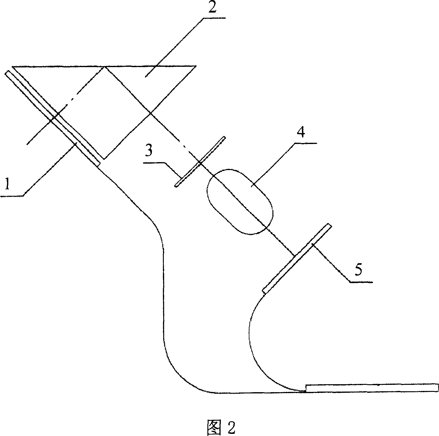
[0026] A kind of collection method of living finger and palm print, referring to Fig. 2, uses a collection device that is made of prism 2, light source 1, lens assembly 4, image sensor 5, and its steps are:
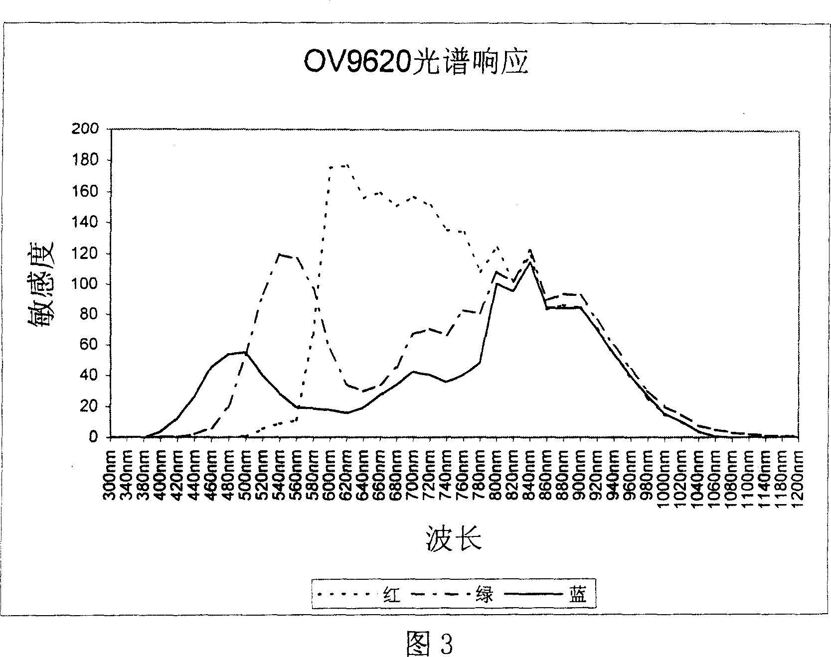
[0027] The light source is an infrared light source, so that the infrared light source emits a monochromatic collection light beam with a wavelength range of 700nm to 1100nm; the infrared light source can use GL4910 infrared light-emitting tube products to form an array; the collection light beam refers to the collection of light emitted by the light source .
[0028] The prism has at least one light beam incident surface for collection, one image output surface, and one collection surface;
[0029] The collection surface of the prism is attached to the living finger and palm to be collected, and a finger and palm print pattern is formed on the collection surface; the so-called living finger and palm refer to human fingers, toes, palms, and soles of feet. The so-called f...
Embodiment 2
[0035] Referring to Fig. 5, Fig. 6, Fig. 7, Fig. 8, a kind of living body finger and palmprint collection device has a housing 10, a collection window 11 is arranged on the top of the housing, a prism 12 is housed on it, and the prism has at least one collection window 10. With beam incidence surface 123, an image output surface 122, a collection surface 121; In said incidence surface one side is provided with infrared light-emitting plate 13, the normal line of this infrared light-emitting plate is orthogonal to collection with beam incidence surface (can also be provided with into a substantially orthogonal state), a lens assembly 14 is arranged on one side of the image output surface, an image sensor 15 is arranged at the output end of the lens assembly, and the optical axis of the lens assembly is orthogonal to the image output surface; the infrared The light emitting board, the lens assembly and the image sensor are installed in the housing. Referring to Fig. 8, the prism...
PUM
| Property | Measurement | Unit |
|---|---|---|
| Wavelength | aaaaa | aaaaa |
Abstract
Description
Claims
Application Information


