Non-volatile memory body and operating method and mfg. method thereof

A technology of manufacturing method and operation method, applied in semiconductor/solid-state device manufacturing, electric solid-state device, semiconductor device, etc., can solve problems such as easy leakage of charge, thermal hole damage of tunnel oxide layer, etc.

Inactive Publication Date: 2007-04-18
MACRONIX INT CO LTD
View PDF0 Cites 0 Cited by
  • Summary
  • Abstract
  • Description
  • Claims
  • Application Information

AI Technical Summary

Problems solved by technology

This article also teaches the method of erasing the memory cell by using the substrate-to-charge-trapping layer-to-band thermoelectric hole tunneling mechanism (BTBHHT). The charge is easy to leak

Method used


Image

  • Non-volatile memory body and operating method and mfg. method thereof
  • Non-volatile memory body and operating method and mfg. method thereof
  • Non-volatile memory body and operating method and mfg. method thereof

Examples


Embodiment Construction

[0029]

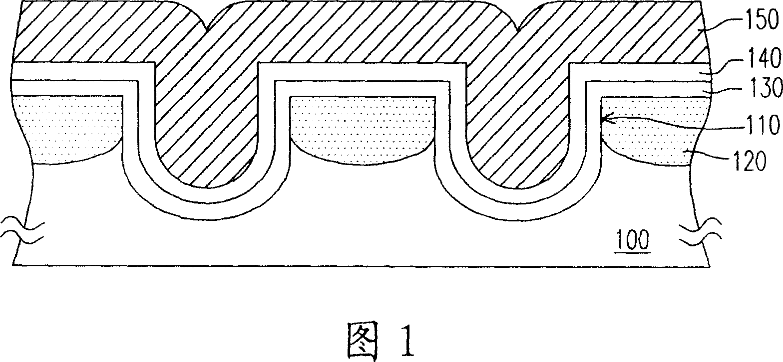
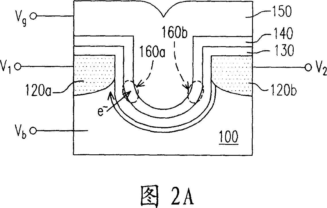
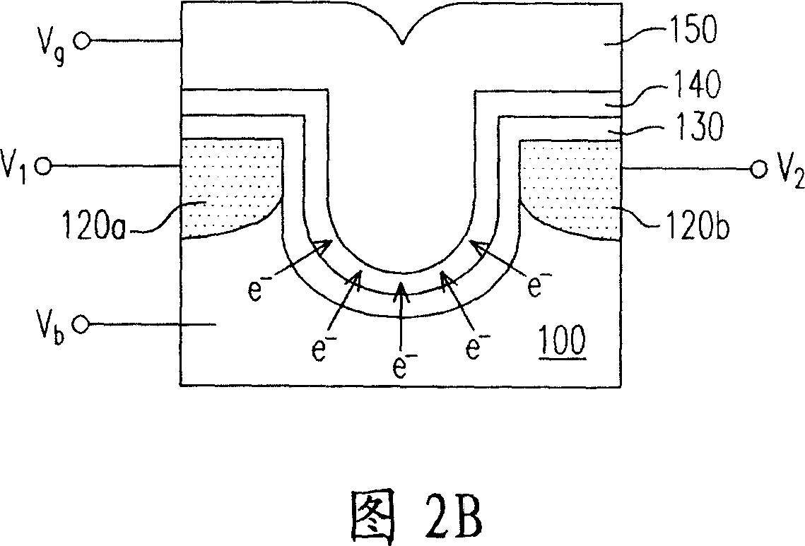
[0030] 1 is a cross-sectional view of a non-volatile memory array structure in a preferred embodiment of the present invention, and FIG. 6F is a top view of the structure, and FIG. 1 corresponds to the IV-IV' section of FIG. 6F. 1 and 6F, the non-volatile memory array at least includes a semiconductor substrate 100 having a plurality of trenches 110, buried bit lines 120, a charge trapping layer 140 and a plurality of word lines 150.

[0031] The aforementioned substrate 100 is, for example, a substrate mainly composed of p-doped silicon, and each trench 110 preferably has a rounded bottom to reduce stress and channel leakage current. The buried bit lines 120 are located in the substrate 100 between the trenches 110 and can be formed by high concentration n-type doping, such as phosphorus ions and / or arsenic ions. The charge trapping layer 140 is disposed on the substrate 100 and in the trench 110, and its material is, for example, SiN, Al 2 o 3 , HfO 2 , HfAlO o...


PUM


Abstract

The invention relates to a nonvolatile memory body and the operating and making methods thereof. And it comprises channeled substrate, charge capturing trap layer in the channel, gate in the channel isolated from the substrate at least through the charge capturing trap layer, and source/drain region in the substrate on two sides of the channel, where the gate material comprises p-doped semiconductor material so as to make it especially suitable to erase the memory body by gate electric hole injection mechanism.

Description

technical field [0001] The present invention relates to a non-volatile memory, and in particular to a non-volatile memory with a charge trapping layer, as well as its operating method and manufacturing method. Background technique [0002] Charge-trapping non-volatile memory has been extensively studied recently because of its simplified manufacturing process and the fact that each memory cell can have more than one storage location. For example, Eitan et al. (IEEE EDL 2000, Vol.21, No.11, 543-545) proposed a local trap type metal oxide semiconductor (MOS) structure binary non-volatile memory cell, which has an n-type The gate electrode and a silicon oxide / silicon nitride / silicon oxide (ONO) compound layer located between the substrate and the gate electrode, wherein the silicon nitride layer is used as a charge trapping layer. However, since the channel length of this kind of memory cell is very small, it will cause serious breakdown leakage and second-bit effect. [0003...

Claims


Application Information

Patent Timeline
Patent Type & Authority Applications(China)
IPC IPC(8): H01L29/78H01L29/43H01L27/105H01L21/336H01L21/8239
Inventor 余昭伦吴昭谊
Owner MACRONIX INT CO LTD
Why Eureka
Try Eureka