Organic electroluminescent device and preparation method thereof

An electroluminescent device and luminescence technology, which is applied in the direction of electric solid-state devices, semiconductor/solid-state device manufacturing, electrical components, etc., can solve the problems of rising operating voltage of light-emitting devices, reduction of luminous efficiency and stability of light-emitting devices, etc.

Inactive Publication Date: 2015-09-02
OCEANS KING LIGHTING SCI&TECH CO LTD +2
View PDF0 Cites 1 Cited by
  • Summary
  • Abstract
  • Description
  • Claims
  • Application Information

AI Technical Summary

Problems solved by technology

Taking the cathode side as an example, electrons must overcome the energy barriers existing at the interface between the cathode and the electron injection layer, between the electron injection layer and the electron transport layer, and between the electron transport layer and the organic light-emitting layer; when a larger When the energy barrier exists at the interface of the above-mentioned layers, electrons are not suitable for entering the organic light-emitting layer, but will accumulate at the interface of each layer. In this way, the operating voltage of the organic electroluminescent device will increase and the lifetime will be reduced.
[0004] In order to avoid the increase of the operating voltage of the organic electroluminescent device, the traditional method is to reduce the thickness of the organic film between the cathode and the organic light-emitting layer, but the thinner the organic film thickness, the lower the luminous efficiency of the organic electroluminescent device. Causes a decrease in stability, and easy to form short circuits and other shortcomings

Method used


Image

  • Organic electroluminescent device and preparation method thereof
  • Organic electroluminescent device and preparation method thereof
  • Organic electroluminescent device and preparation method thereof

Examples


preparation example Construction

[0032] The present invention also provides a preparation method for the above-mentioned organic electroluminescent device, the steps of which are:

[0033] a ) Pre-treatment of anode conductive substrate

[0034] Use ITO glass (that is, indium tin oxide transparent conductive glass) as the anode conductive substrate, and wash it with detergent, deionized water, acetone and ethanol successively, and clean it with an ultrasonic cleaner. , stop for 5 minutes, repeat the method 3 times, and then dry it in an oven for use; the cleaned ITO glass also needs surface activation treatment to increase the oxygen content on the surface of the ITO glass and improve the ITO glass. The work function of the surface; the thickness of ITO glass is 100-150nm;

[0035] b) Preparation of the first hole injection layer

[0036] Using N,N'-diphenyl-N,N'-di(1-naphthyl)-1,1'-biphenyl-4,4'-diamine (NPB), 4,4',4'' -Tris(carbazol-9-yl)triphenylamine (TCTA), 4,4'-bis(9-carbazole)biphenyl (CBP), N,N'-b...

Embodiment 1

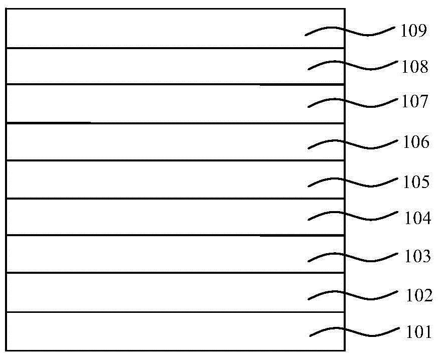
[0053] Such as figure 1 As shown, the present embodiment 1 provides an organic electroluminescent device, the organic electroluminescent device has a layered structure, and the organic electroluminescent device includes in sequence: an anode conductive substrate 101, a first hole injection layer 102 , a hole transport layer 103 , a blue light emitting layer 104 , an electron transport layer 105 , a first electron injection layer 106 , a second hole injection layer 107 , a second electron injection layer 108 and a cathode layer 109 .

[0054] The specific expression of the organic electroluminescent device is: ITO glass / MoO 3 :NPB(30:100) / NPB / FIrpic:CBP(5:100) / Bphen / Cs 2 CO 3 :Bphen(30:100) / MoO 3 :NPB(30:100) / Cs 2 CO 3 :Bphen(30:100) / Ag, wherein, the colon ":" indicates that the former is doped in the latter.

[0055] The present embodiment 1 also provides the preparation method of the above-mentioned organic electroluminescence device, and its steps are:

[0056] a) Pre...

Embodiment 2

[0075] Such as figure 1 As shown, this embodiment 2 provides an organic electroluminescent device, the organic electroluminescent device is a layered structure, and the organic electroluminescent device includes in sequence: an anode conductive substrate 101, a first hole injection layer 102 , a hole transport layer 103, a blue light emitting layer 104, an electron transport layer 105, a first electron injection layer 106, a second hole injection layer 107, a second electron injection layer 108, and a cathode layer 109.

[0076] The specific expression of the organic electroluminescent device is: ITO glass / WO 3 :TCTA(25:100) / TCTA / FIr6:mCP(20:100) / BCP / CsF:BCP(25:100) / WO 3 :TCTA(25:100) / CsF:BCP(25:100) / Al, wherein the colon ":" indicates that the former is doped in the latter.

[0077] This embodiment 2 also provides the preparation method of the above-mentioned organic electroluminescence device, and its steps are as follows:

[0078] a) Pretreatment of the anode conductive ...


PUM


Abstract

The invention relates to an organic electroluminescent device and a preparation method thereof, wherein the organic electroluminescent device has a layered structure and comprises an anode conductive substrate, a first hole injection layer, a hole transport layer, a blue light emitting layer, an electronic transmission layer, a first electron injection layer, a second hole injection layer, a second electron injection layer and a cathode layer; wherein the anode conductive substrate, the first hole injection layer, the hole transport layer, the blue light emitting layer, the electronic transmission layer, the first electron injection layer, the second hole injection layer, the second electron injection layer and the cathode layer are successively laminated. The first hole injection layer and the second hole injection layer are made of hole injection material and p-type material which is doped into the hole injection material. The first electron injection layer and the second electron injection layer are made of electron injection material and n-type material which is doped into the electron injection material. According to the organic electroluminescent device, through the added second hole injection layer and the second electron injection layer, working voltage can be reduced and luminous efficiency can be improved effectively.

Description

technical field [0001] The invention relates to the field of optoelectronic devices, in particular to an organic electroluminescent device and a preparation method thereof. Background technique [0002] Organic electroluminescent devices (OLEDs) have some unique advantages: (1) OLEDs are diffuse surface light sources, and do not require an additional light guide system to obtain large-area white light sources like light-emitting diodes (LEDs); (2) Due to the diversity of organic light-emitting materials, OLED lighting can design the required color of light according to needs. At present, both small molecule OLEDs and polymer organic light-emitting diodes (PLEDs) have obtained all colors of light including the white light spectrum. ; (3) OLED can be made on a variety of substrates such as glass, ceramics, metal, plastic and other materials, which makes the design of lighting sources more free; (4) OLED lighting panels can be made in the way of making OLED displays. (5) OLED ...

Claims


Application Information

Patent Timeline
Patent Type & Authority Applications(China)
IPC IPC(8): H01L51/50H01L51/54H01L51/56
Inventor 周明杰钟铁涛王平冯小明
Owner OCEANS KING LIGHTING SCI&TECH CO LTD
Why Eureka
Try Eureka