

Photoelectric conversion substrate
A photoelectric conversion and substrate technology, which is applied in the direction of optical waveguide and light guide, can solve the problem of incompatibility between photoelectric conversion substrate and printed circuit board process, and achieve the effect of improving displacement tolerance, reducing production cost and increasing displacement tolerance
- Summary
- Abstract
- Description
- Claims
- Application Information
AI Technical Summary
Problems solved by technology
Method used
Image

Examples
Embodiment 1
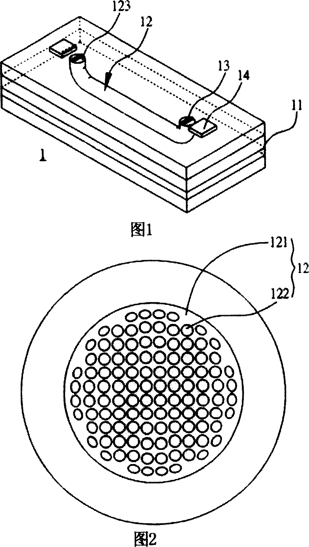
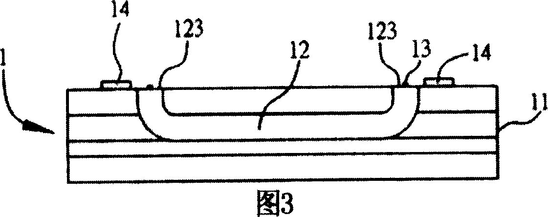
[0036] 3 is a cross-sectional view of Embodiment 1 of the photoelectric conversion substrate 1 of the present invention. The two end faces 123 of the at least one honeycomb micro-optical waveguide 12 each have at least one pair of alignment structures or alignment marks (not marked), wherein the At least one pair of alignment structures or alignment marks are aligned and optically connected to the photoelectric element 13, so that the displacement tolerance of the photoelectric element 13 on the package of the photoelectric conversion substrate 1 and the number of array channels can be increased, and in The end face 123 of the honeycomb micro-optical waveguide 12 has an asymmetric structure, which is beneficial to the alignment during wiring. Since this structure is applied under the structure of an M×N array, in order to avoid the When the structure is twisted during wiring, the 1-to-1 correspondence between the Tx Channel and the Rx Channel is misplaced. The asymmetric struct...
Embodiment 2
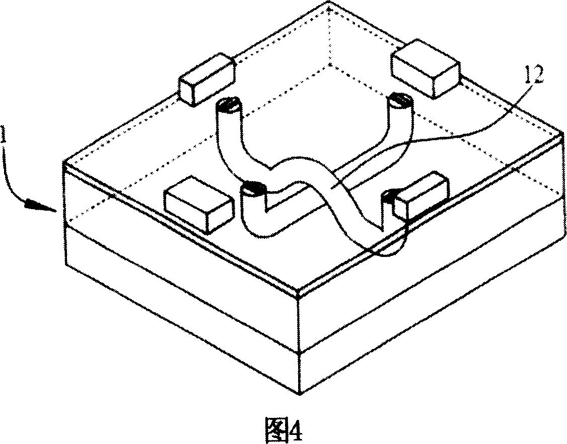
[0039] Fig. 4 is a schematic diagram of Embodiment 2 of the photoelectric conversion substrate 1 of the present invention, where the difference from Fig. 1 is that the photoelectric conversion substrate 1 of the present invention has a plurality of honeycomb micro-optical waveguides 12, wherein the honeycomb micro-optical waveguides 12 are connected to each other It can cross each other, it can realize three-dimensional multi-channel structure and because the structure of the honeycomb micro-optical waveguide 12 can allow more channel transmission per unit area, it is not limited by the Pitch 250mm of the optical fiber, so in The pitch of the VCSEL element can be less than 250mm. In other words, there can be more VCSEL elements per unit area on the VCSEL wafer.
Embodiment 3
[0041] Please refer to FIG. 5, which is a schematic diagram of Embodiment 3 of the photoelectric conversion substrate 1 of the present invention. The difference from FIG. The photoelectric conversion substrate 1 of the optical waveguide 12, wherein the optical component sub-module 2 integrates a photoelectric component and an IC driving component.
[0042] In summary, the structure of the photoelectric conversion substrate 1 disclosed by the present invention is easy to manufacture, can reduce production costs, overcomes the problem of incompatibility between existing photoelectric conversion substrates and printed circuit boards, and can effectively increase the number of photoelectric elements in the photoelectric conversion substrate. Displacement tolerance on the package.
PUM
 Abstract
Description
Claims
Application Information