Around exposure device and method thereof

An exposure method and an exposure device technology, which are applied in photolithography exposure devices, microlithography exposure equipment, laser welding equipment, etc., can solve problems such as structural integration, exposure speed impact, substrate surface contamination, etc.

Inactive Publication Date: 2007-05-09
ORC MFG
View PDF0 Cites 10 Cited by
  • Summary
  • Abstract
  • Description
  • Claims
  • Application Information

AI Technical Summary

Problems solved by technology

[0017] However, in the respective exposure devices, since the absolute position is positioned when the alignment work of the substrate is performed, the references of the respective alignment work are different, and the structure cannot be easily integrated.
[0018] (2) Moreover, when the exposure process of the identification mark and the exposure process of the surrounding area are continuously performed, the moving speed of the substrate will affect the exposure speed of any exposure process.
However, as in Patent Document 4, when the irradiated exposure light expands or contracts symmetrically with respect to the center of the optical path, it cannot co

Method used


Image

  • Around exposure device and method thereof
  • Around exposure device and method thereof
  • Around exposure device and method thereof

Examples


Embodiment Construction

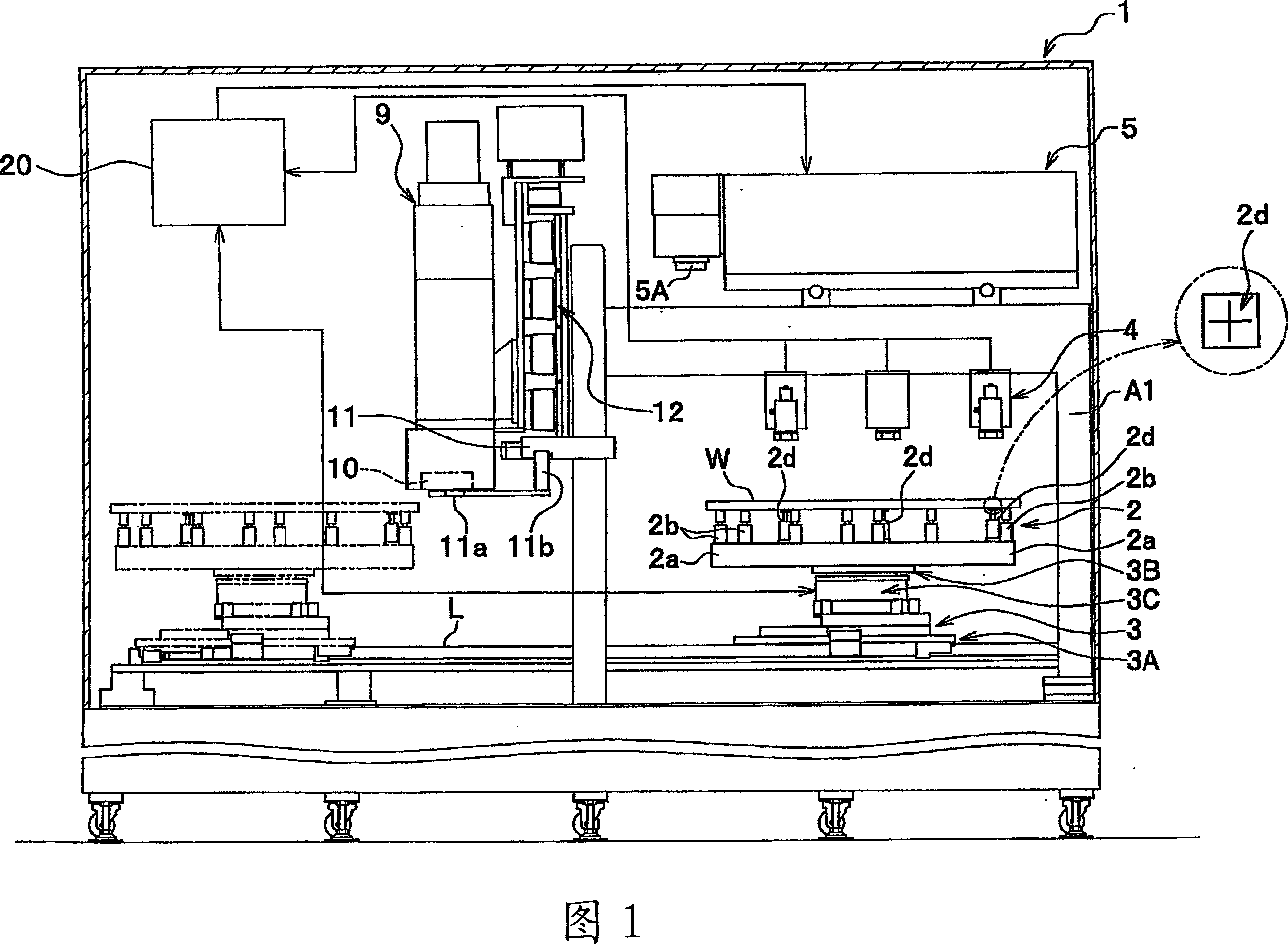
[0127] Hereinafter, the best mode of the laser beam and ultraviolet irradiation peripheral exposure apparatus and its method for carrying out the present invention will be described with reference to the drawings.

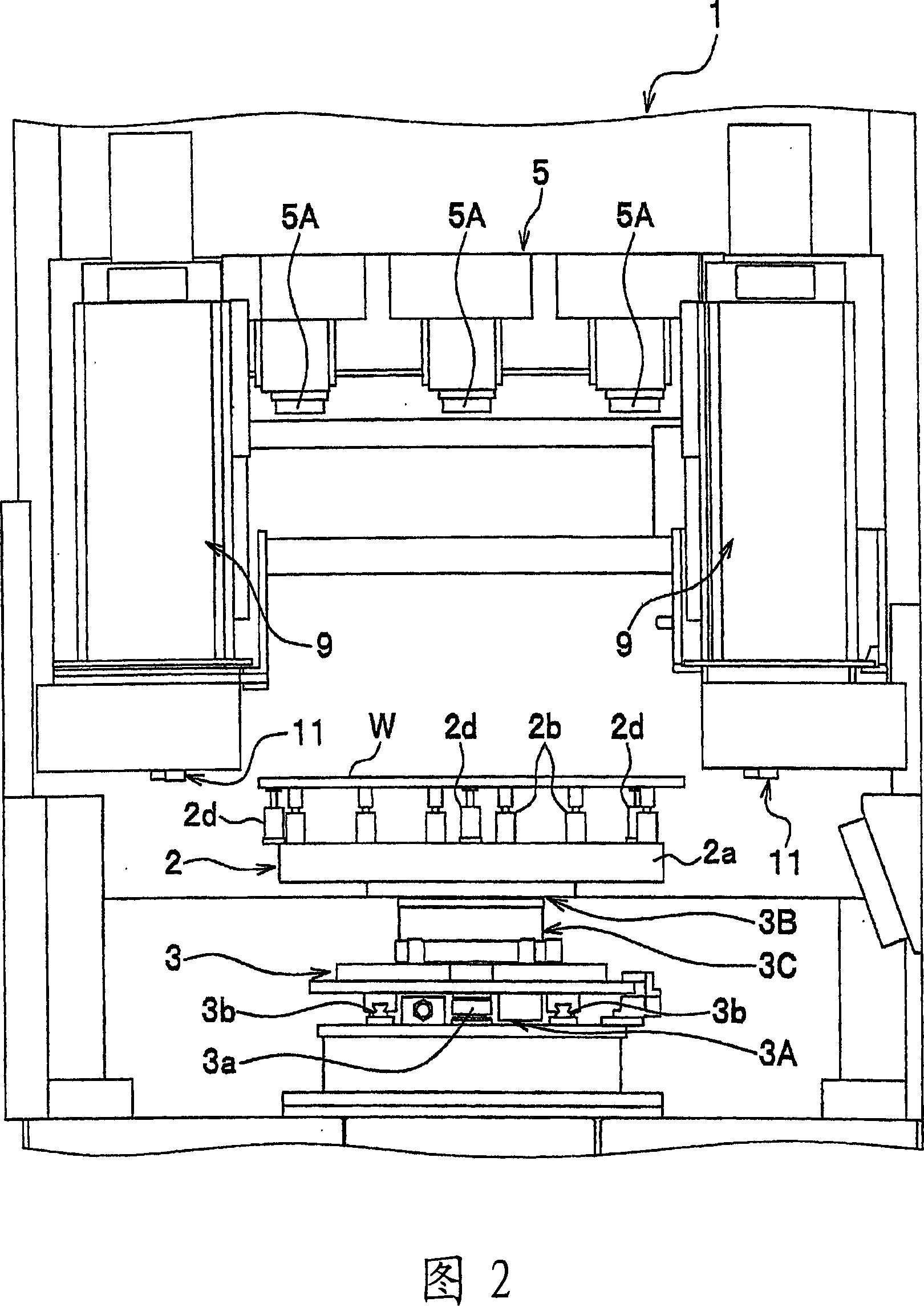
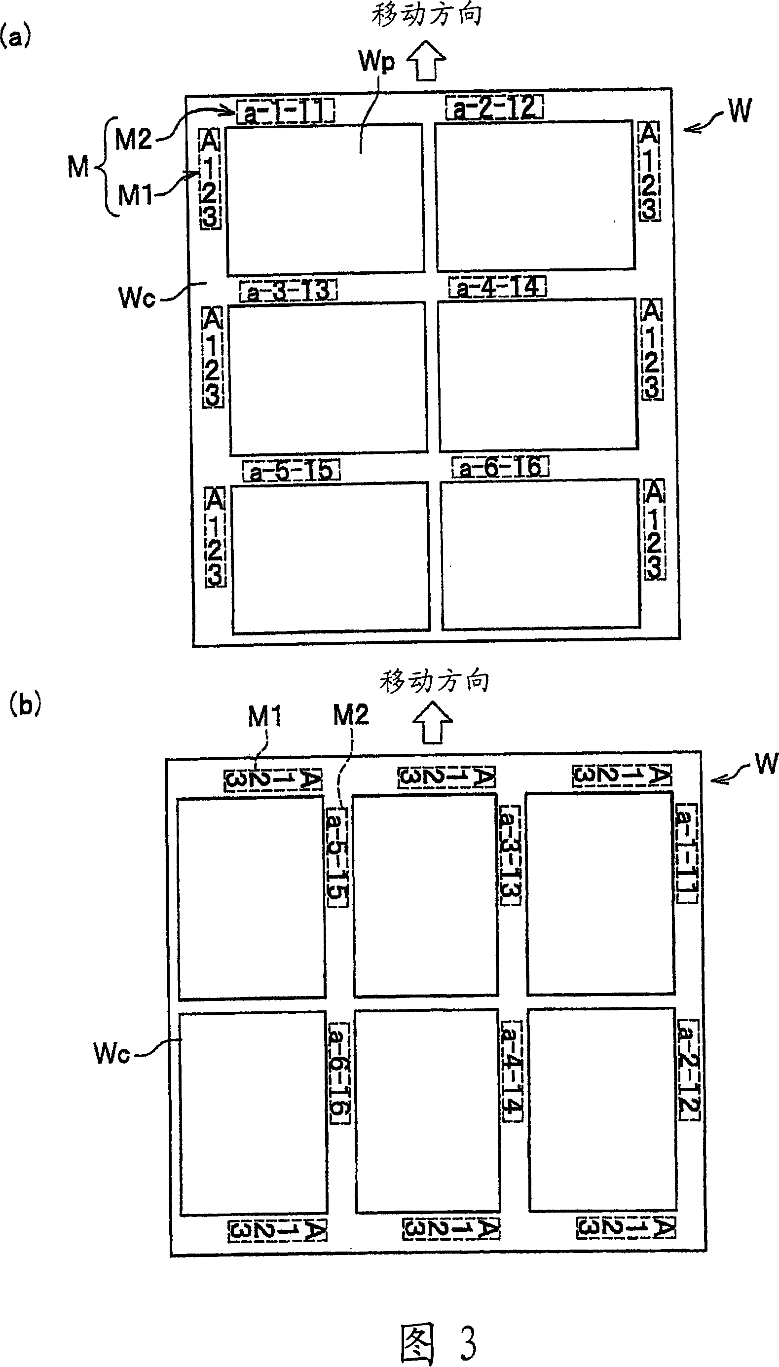
[0128] Fig. 1 is a cross-sectional view schematically showing the inside of the device from the side direction without omitting the laser beam and part of the ultraviolet ray irradiation peripheral exposure device; Sectional view in the device; Fig. 3 (a), (b) is a top view showing an example of a substrate used in a laser beam, ultraviolet irradiation peripheral exposure device; Fig. 4 is a plan view showing a laser beam, ultraviolet irradiation peripheral exposure device Side view of the pedestal.

[0129] As shown in FIG. 1 , a laser beam and ultraviolet irradiation peripheral exposure device (hereinafter referred to as the device) 1 mainly includes: a pedestal 2 for holding a loaded substrate W; An imaging device 4 for photographing; a moving transport mechani...


PUM


Abstract

The present invention provides a peripheral exposure device and method thereof which can form an identification mark in any position of peripheral region and minimize the substrate surface staining factor. The peripheral exposure device comprises an ultraviolet irradiation unit 9 on the moving path which irradiates the light containing ultraviolet on the peripheral region of the substrate through an irradiation opening and an irradiation lens, and an occluder adjusting mechanism 10 in the irradiation region, which can control the occluder in manner of shading at least part of the irradiation opening 9m to shade the identification mark according to the moving speed of the substrate.

Description

technical field [0001] The present invention relates to a peripheral exposure device and method thereof, which irradiate the peripheral region with ultraviolet light while shielding identification marks such as marks and characters formed in the peripheral region formed around a pattern region of a substrate. light for peripheral exposure. Background technique [0002] Generally speaking, regarding a substrate to be exposed with a pattern in an exposure device, for example, in a liquid crystal substrate, a substrate with a size of about 500mm x 500mm was processed at that time, and a substrate with a large size of 2160mm x 2460mm is now being enlarged. to process. This large substrate is cut and separated into predetermined individual substrate pieces to manufacture a substrate mounted on a general image receiving device. When the substrate is cut and separated from a large state, in order to manage it and the management of the manufacturing process, the laser beam is used...

Claims


Application Information

Patent Timeline
IPC IPC(8): G03F7/20B23K26/00G03B17/48
Inventor 剑持晴康佐藤博明池田泰人森昌人
Owner ORC MFG
Why Eureka
Try Eureka