Method for fabricating grid dielectric layer, and semiconductor components

A manufacturing method and a technology for a gate dielectric layer, which are applied in the fields of semiconductor/solid-state device manufacturing, semiconductor devices, electrical components, etc., and can solve problems such as the inability to increase the on-state current of semiconductor components.

Inactive Publication Date: 2007-05-09
UNITED MICROELECTRONICS CORP
View PDF0 Cites 0 Cited by
  • Summary
  • Abstract
  • Description
  • Claims
  • Application Information

AI Technical Summary

Problems solved by technology

In the case of narrow gate width, the method of fabricating the gate dielectric layer in the prior art cannot increase the on-state current of the semiconductor element

Method used


Image

  • Method for fabricating grid dielectric layer, and semiconductor components
  • Method for fabricating grid dielectric layer, and semiconductor components
  • Method for fabricating grid dielectric layer, and semiconductor components

Examples


Embodiment Construction

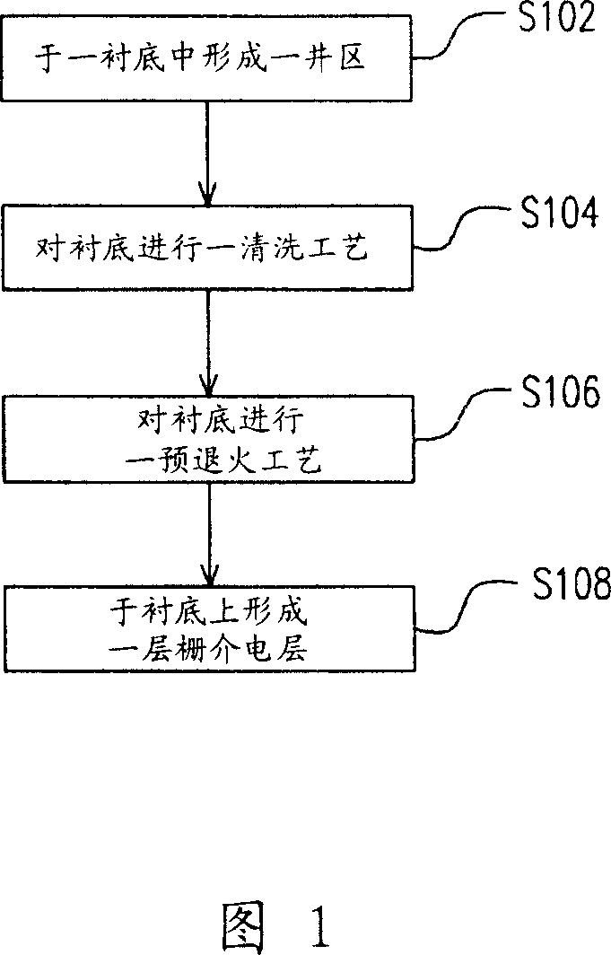
[0039] FIG. 1 is a flowchart illustrating the fabrication of the gate dielectric layer proposed by the present invention.

[0040] First, a well region is formed in a substrate (S102). Next, a cleaning process is performed on the substrate (S104). Then, a pre-annealing process is performed on the substrate (S106). Next, a gate dielectric layer is formed on the substrate (S108).

[0041] The gate dielectric layer formed according to the above method, because the pre-annealing process is performed after the native oxide layer is removed by the cleaning process, can effectively compensate for the lattice defects caused by the ion implantation process. In this way, the formed gate oxide layer has better quality and can effectively increase the on-state current of the semiconductor device.

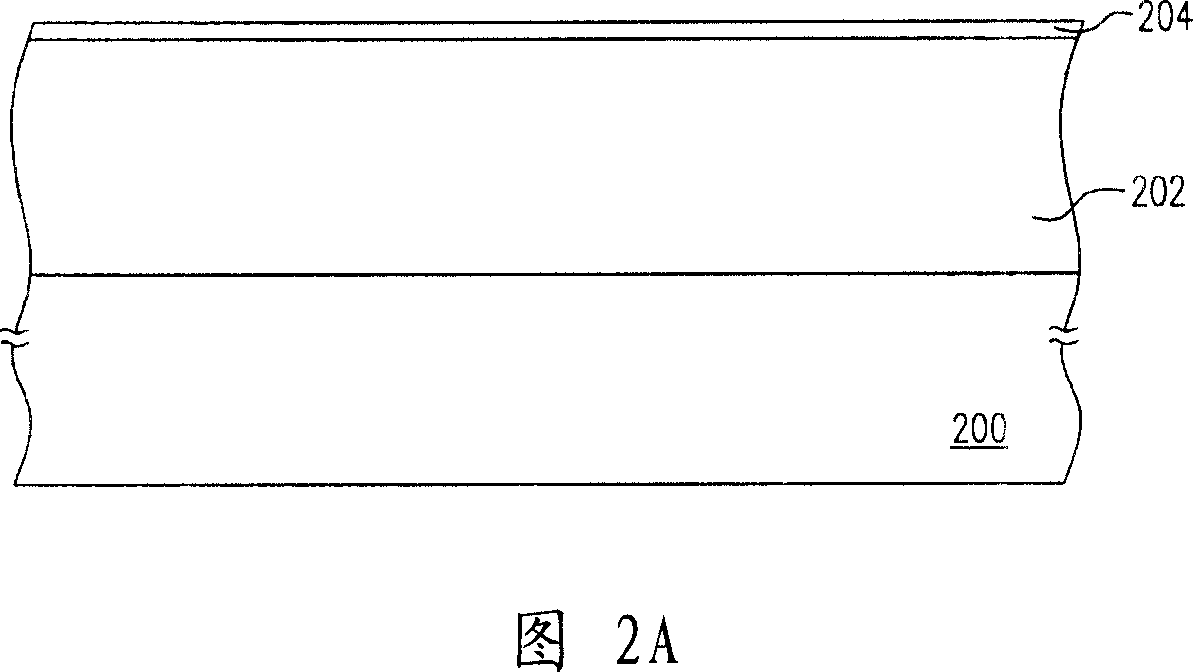
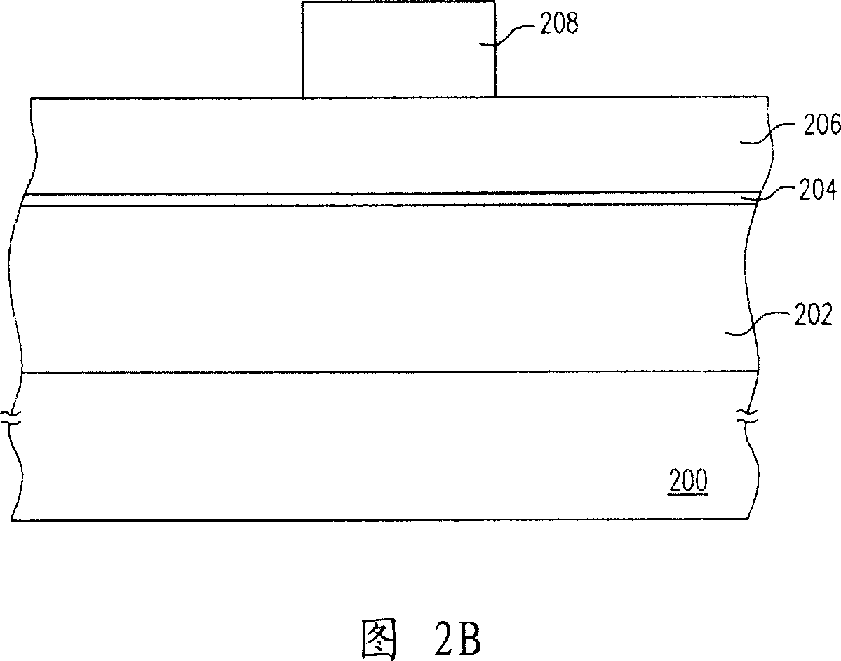
[0042] 2A-2D are cross-sectional views of a manufacturing process of a semiconductor device according to an embodiment of the present invention.

[0043] Please refer to FIG. 2A , the semic...


PUM


Abstract

The method for manufacturing grating dielectric layer includes steps: first, forming a well area on substrate; next, carrying out a cleaning procedure for the substrate; then, carrying out a pre annealing process for the substrate; finally, forming a layer of grating dielectric layer on the substrate. The invention raises current in open state of semiconductor element.

Description

technical field [0001] The invention relates to a gate dielectric layer and a manufacturing method of a semiconductor element, in particular to a gate dielectric layer and a semiconductor element manufacturing method capable of improving the operation performance of the semiconductor element. Background technique [0002] In the current prior art, the method of manufacturing the gate dielectric layer of the metal oxide semiconductor device first forms a well region in a substrate by ion implantation. Next, a rapid thermal annealing process is performed on the substrate to compensate for lattice defects generated during ion implantation. Then, a cleaning process is performed, and a gate dielectric layer is formed on the substrate. [0003] However, the rapid thermal annealing process is performed before the cleaning process. If the native oxide layer has not been removed by the cleaning process, the compensation effect on the lattice defects is poor, and the gate dielectric ...

Claims


Application Information

Patent Timeline
IPC IPC(8): H01L21/28H01L21/31H01L21/336
Inventor 郑礼贤李东兴郑子铭沈泽民邱大秦
Owner UNITED MICROELECTRONICS CORP
Why Eureka
Try Eureka