Composition of a solder, and method of manufacturing a solder connection

A technology of composition and solder, applied in the direction of welding equipment, welding medium, welding/cutting medium/material, etc., can solve the problems of increased complexity and poor solderability

Active Publication Date: 2007-05-09
LUMILEDS HLDG BV +1
View PDF3 Cites 4 Cited by
  • Summary
  • Abstract
  • Description
  • Claims
  • Application Information

AI Technical Summary

Problems solved by technology

Such an adhesive layer needs to be provided separately, which involves additional processing steps and additional costs
Furthermore, this adhesion layer limits the use of this poorly solderable metal, especially in components and carriers that need to withstand a certain minimum temperature
The problem is compounded in contacts of a first substrate that comprise a different metal than contacts of a second substrate facing the first substrate.

Method used


Image

  • Composition of a solder, and method of manufacturing a solder connection
  • Composition of a solder, and method of manufacturing a solder connection
  • Composition of a solder, and method of manufacturing a solder connection

Examples


Embodiment Construction

[0049] The drawings are not drawn to scale, and the same reference numbers in different drawings refer to the same parts.

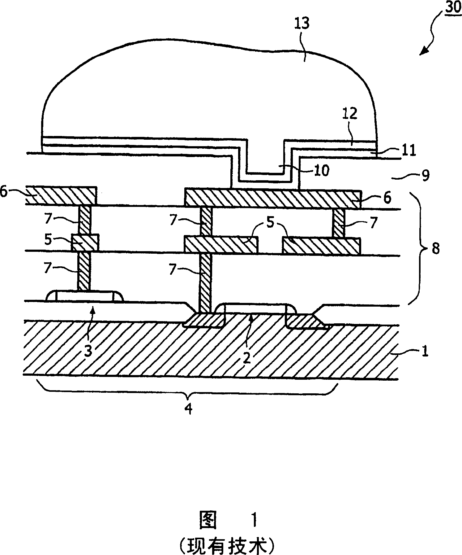
[0050] Figure 1 shows a schematic cross-sectional view of a prior art substrate. The substrate is an integrated circuit device. It includes multiple elements, in this case MOS transistor 2 and polysilicon track 3. The circuit is provided in an active circuit area 4 on the surface of the semiconductor body 1. In the coverage relationship related to the circuit devices 2, 3, an interconnection structure 8 is provided for interconnecting the circuit devices 2, 3 to form a circuit. In this embodiment, the interconnection structure 8 includes a first patterned metal layer 5, a second patterned metal layer 6 and an interconnection via 7. In this example, the patterned metal layers 5, 6 include aluminum or aluminum alloy, such as AlCu. A layer of passivation material 9 is arranged on the interconnect structure 8. The passivation material is for example silicon nitri...


PUM

PropertyMeasurementUnit
The average diameteraaaaaaaaaa

Abstract

The solder composition comprises particles of a thermodynamically metastable alloy. One of the elements of the alloy will form an intermetallic compound with a metal surface. The solder composition is particularly suitable for use in bumping of semiconductor devices.

Description

Technical field [0001] The present invention relates to a solder composition. [0002] The present invention also relates to a method for preparing a conductive connection between the soldering area of ​​the first substrate and the soldering area of ​​the second substrate through the solder composition, which includes the following steps: [0003] Providing a solder composition on the soldering area of ​​the first substrate; [0004] Combining the first and second substrates such that the solder composition is sandwiched between the soldering areas of the first and second substrates, and [0005] The conductive connection is provided by heating the solder composition. [0006] The present invention also relates to a substrate with a soldering area on which there is a layer of solder composition. The present invention also relates to a component comprising a first and a second substrate with a soldering area, connected by conductive solder. The bonding areas of one and the second s...

Claims


Application Information

Patent Timeline
IPC IPC(8): B23K35/02B23K35/26B23K35/28H05K3/34
CPCB23K35/0222B23K35/264H01L2224/29109H01L2224/2919B23K35/286H01L2924/0133H01L2224/32245H01L2224/48247H05K3/3484B23K35/262H01L24/29H01L2924/01327H01L2924/01322H01L2924/01029H01L2224/29111H01L2924/0132H01L2224/73265H01L2224/48464H05K2201/0215H01L2924/13091H01L2924/14H01L2924/181Y10T428/1216Y10T428/12028Y10T428/24826Y10T428/31678B23K35/24B23K35/26B23K35/28H05K3/3485H01L2924/00H01L2924/0105H01L2924/01013H01L2924/01047H01L2924/0103H01L2924/01049H01L2924/01082H01L2924/01083H01L2924/00014H01L2924/3512H01L2924/00012B23K35/22B23K35/02H05K1/14
Inventor N·J·A·范维恩M·H·比格拉里
Owner LUMILEDS HLDG BV
Why Eureka
Try Eureka