

Pixel array, display panel thereof and display
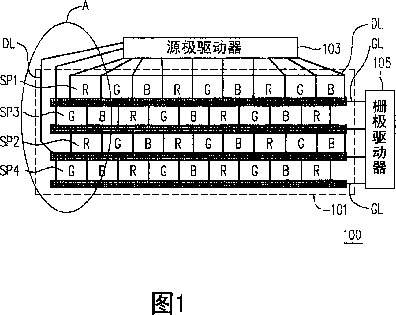
A technology of pixel array and display panel, which is applied in static indicators, instruments, nonlinear optics, etc., can solve the problems of decreased transmittance of display panel 101, increased product manufacturing cost, decreased aperture ratio, etc., so as to improve transmittance. , the effect of reducing the load and reducing the size
- Summary
- Abstract
- Description
- Claims
- Application Information
AI Technical Summary
Problems solved by technology
Method used
Image

Examples
no. 1 example
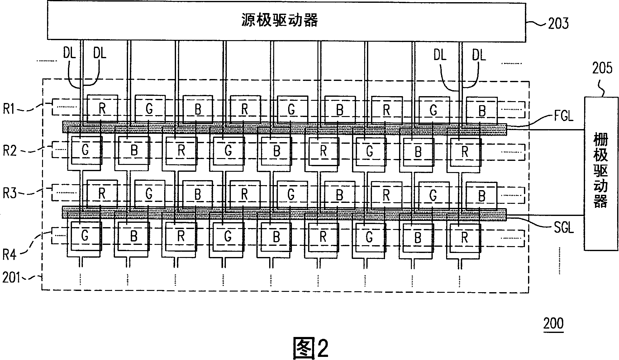
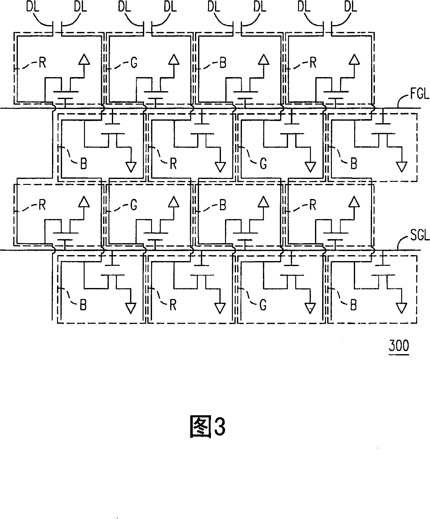
[0046] 2 is a block diagram of a display 200 according to the first embodiment of the present invention, wherein the display 200 can be any flat display, such as liquid crystal display (liquid crystal display, LCD), plasma display (plasma display panel, PDP) and so on. Referring to FIG. 2 , the display 200 is a liquid crystal display, which includes a display panel 201 , a source driver 203 , and a gate driver 205 . Wherein, the display panel 201 includes a pixel array (pixel array), which is disposed on a substrate (not shown), and has a first scanning line FGL, a second scanning line SGL, and several data lines DL. In this first embodiment, the scan line FGL is electrically connected to the sub-pixel R1 of the first column and the sub-pixel R2 of the second column, and the scan line SGL is electrically connected to the sub-pixel R3 of the third column and the sub-pixel R4 of the fourth column, and the above-mentioned Sub-pixels in adjacent columns of the four columns of sub-...
no. 2 example
[0057] FIG. 4 is a block diagram of a display 400 according to a second embodiment of the present invention. Please refer to FIG. 2 and FIG. 4 together. The biggest difference between the display 400 and the display 200 is that the data lines DL of the first group and the data lines DL of the second group of the pixel array of the display panel 401 are pulled in different ways. The drawing method of the data lines DL of the first group and the data lines DL of the second group in the pixel array of the display panel 201 is the same as that of the display 200 in terms of the effects to be achieved and the problems to be solved, so no further To repeat.
[0058] In this second embodiment, the data lines DL of the first group go leftward along the right side of each sub-pixel in the first row of sub-pixels R1 to the bottom and are connected to the corresponding sub-pixels in the first row of sub-pixels R1 electrically connected, and surround the left side of the sub-pixels in th...
no. 3 example
[0062] FIG. 6 is a block diagram of a display 600 according to a third embodiment of the present invention. Please refer to FIG. 2 and FIG. 6 together. The biggest difference between the display 600 and the display 200 is that the data lines DL of the pixel array of the display panel 601 are divided into six groups, and the way of pulling the lines is also different from that of the pixels of the display panel 201. The data line DL drawing method of the array, but the effect to be achieved and the problems to be solved are the same as those of the display 200 , so it will not be repeated here.
[0063] In this third embodiment, the data lines DL of the first group go leftward along the right side of the sub-pixels in the corresponding first row of sub-pixels R1 to the bottom and are connected to the sub-pixels in the corresponding first row of sub-pixels R1 electrically connected, and surround the left side of the sub-pixels in the corresponding adjacent non-aligned second col...
PUM
 Abstract
Description
Claims
Application Information