Static discharge protection structure, element and manufacturing of element

A technology for electrostatic discharge protection and electrostatic discharge, which is applied in the direction of static indicators, instrument parts, shielding, etc., and can solve problems such as damage, lack of components on the display, and inability to effectively release energy.

Inactive Publication Date: 2007-05-30
AU OPTRONICS CORP
View PDF0 Cites 4 Cited by
  • Summary
  • Abstract
  • Description
  • Claims
  • Application Information

AI Technical Summary

Problems solved by technology

With the development of technology, today's display integrates the driving circuit and the thin film transistor, which means that the driving circuit and the thin film transistor are formed on the same substrate; when the driving circuit and the thin film transistor are integrated, the conventional structure cannot provide electrostatic discharge protection for the driving circuit , so electrostatic discharge energy can cause damage to the drive circuit on the display
[0006] In addition, when the turn-on voltage of the designed ESD protection element is not high enough, the operating voltage applied to the thin film transistor will cause the ESD protection element connected to the thin film transistor to Leakage current
Since the conventional ESD protection architecture is to place a large number of ESD protection components around the thin film pixel array, the leakage current will affect the normal operation of the display
When the conduction voltage of the electrostatic discharge protection components is too high, when the display is subjected to electrostatic discharge, the electrostatic discharge current discharges through a high-resistance path, which cannot effectively release energy, resulting in damage to the components on the display.
[0007] As can be seen from the above description, there is still a lack of an ESD protection architecture that can provide good protection for liquid crystal displays that integrate drive circuits and thin film transistors, and at the same time prevent the leakage current of ESD protection components from affecting the normal operation of the display.

Method used


Image

  • Static discharge protection structure, element and manufacturing of element
  • Static discharge protection structure, element and manufacturing of element
  • Static discharge protection structure, element and manufacturing of element

Examples


Embodiment Construction

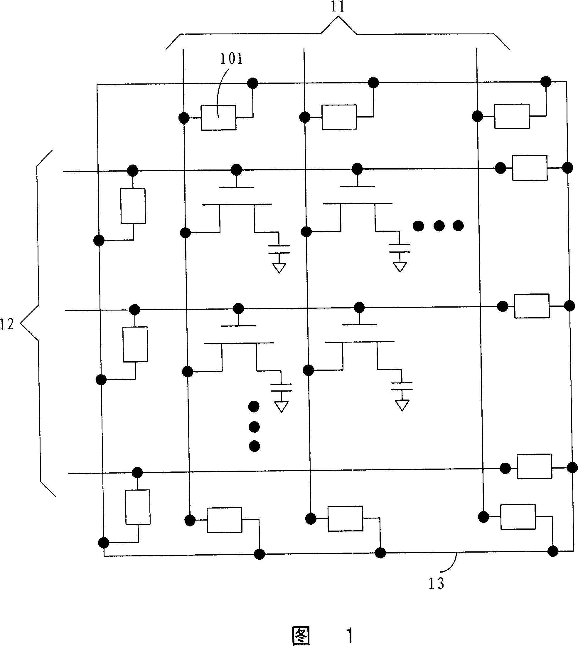
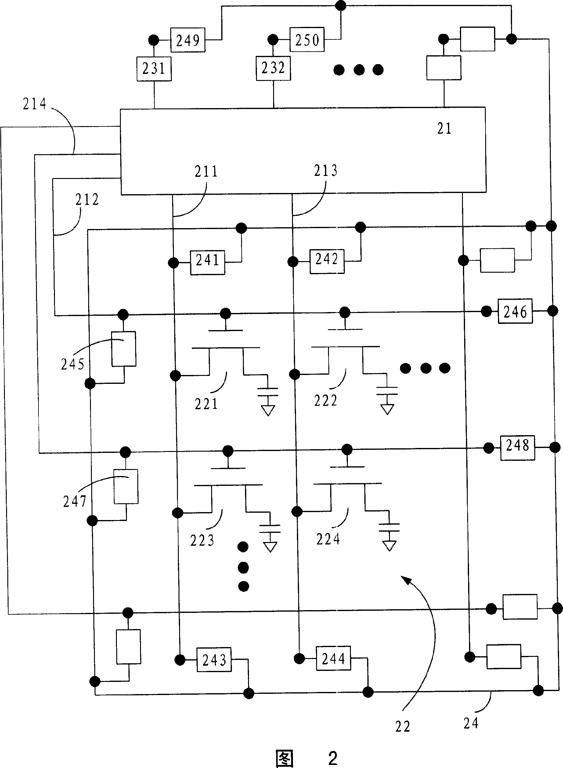
[0019] FIG. 2 shows a first embodiment of the present invention, which provides an electrostatic discharge protection structure between the integrated driving circuit 21 and the pixel array 22 . The output terminal of the driving circuit is respectively connected to the gate and source / drain of each thin film transistor in the pixel array 22 . In FIG. 2 , only a schematic diagram of connection between a part of the pixel array 22 and the driving circuit 21 is shown. The data lines 211 are connected to the pixel array, and are arranged as source / drain electrodes of a plurality of thin film transistors in a row. In FIG. 2 , only a part of the thin film transistors 221 and the thin film transistors 223 connected to the data lines 211 are shown. Similarly, the sources / drains of the TFTs 222 and 224 are connected to the data line 213 . Gates of the thin film transistor 221 and the thin film transistor 222 are connected to the gate line 212 . Gates of the thin film transistor 223 ...


PUM


Abstract

The invention discloses a static discharge protector, static discharge safeguard structure and a method for making static discharge protector. The static discharge protector includes at least four ionic doping areas that the two adjacent doping areas are in different type. The static discharge safeguard structure includes a static discharge collecting bar; many the first static discharge protectors are connected with the grid of thin film transistor of a display and the static discharge collecting bar; many the second static discharge protectors are connected with the drain / source of thin film transistors and the static discharge collecting bar; many the third static discharge protectors are connected with the output and input of one drive circuit of display and the static discharge collecting bar.

Description

【Technical field】 [0001] The invention relates to an electrostatic discharge protection framework and components. More specifically, it relates to an ESD protection structure and components for providing ESD protection in a liquid crystal display. 【Background technique】 [0002] Electrostatic discharge (electrostatic discharge) discharges electrostatic energy into an electronic circuit, resulting in sudden short-term high voltage and high current in the circuit. These high voltages and high currents may cause damage to electronic circuits, including damage to internal circuits, damage to internal wires, and the like. Therefore, providing ESD protection between multiple internal circuits and the pixel array becomes a problem to be solved. [0003] When electrostatic discharge occurs, a large amount of heat will be generated in a short time due to its high voltage and high current. In a liquid crystal display, since the substrate is made of glass and has a low thermal condu...

Claims


Application Information

Patent Timeline
IPC IPC(8): G02F1/133G12B17/02
Inventor 柯明道邓至刚孙文堂
Owner AU OPTRONICS CORP
Why Eureka
Try Eureka