A TFT LCD pixel structure

A pixel structure and pixel electrode technology, applied in nonlinear optics, instruments, optics, etc., can solve the problems of reducing device aperture ratio, TFT pixel electrode damage, high pressure, etc., to increase the aspect ratio and increase the on-state current Effect

Active Publication Date: 2007-05-30
BOE TECH GRP CO LTD +1
View PDF0 Cites 8 Cited by
  • Summary
  • Abstract
  • Description
  • Claims
  • Application Information

AI Technical Summary

Problems solved by technology

In the design of large-scale devices, it is hoped to increase the width-to-length ratio (W / L) to better meet the charging rate requirements. This will increase the width of the conductive channel (channel), increase the size of the TFT, and reduce the Aperture ratio of the device
[0005] 2. This kind of structural design is more complicated, and there are many factors to be considered
[0006] 3. More importantly, based on the design of this kind of TFT device structure, taking the form of the columnar spacer (PS) of the color filter (CF) on the TFT as an example, the columnar spacer (PS) is vulnerable to damage Damage, forming problems such as box thickness (Gap) and picture defects (mura)
[0007] In general design, the top size (top size) of the cylindrical spacer (PS) is smaller than the bottom size (bottom size), which is approximately a trapezoidal cone structure. After the box alignment process, the upper end of the cylindrical spacer (PS) has a certain As shown in the circular area in Figure 2, when the panel surface is subjected to external force, the color filter substrate is easy to move relative to the array substrate, and because the contact surface between the columnar spacer (PS) and the TFT is in the On the ridges of the source and drain (S / D), the unevenness of the surface is likely to cause damage to the upper end surface of the columnar spacer (PS). At the same time, because the two are not in surface contact, the pressure on the contact end will be very large. This may also cause damage to the TFT pixel electrode (ITO), as shown in Figure 3
[0008] 4. At the same time, this design cannot well limit the movement of the upper end of the column spacer (PS) on the array substrate (array). Under the action of external force, the slight movement of the color filter (CF) will exceed the The upper limit of the specification may cause white mura or zaratsuki light leakage

Method used


Image

  • A TFT LCD pixel structure
  • A TFT LCD pixel structure
  • A TFT LCD pixel structure

Examples


Embodiment 1

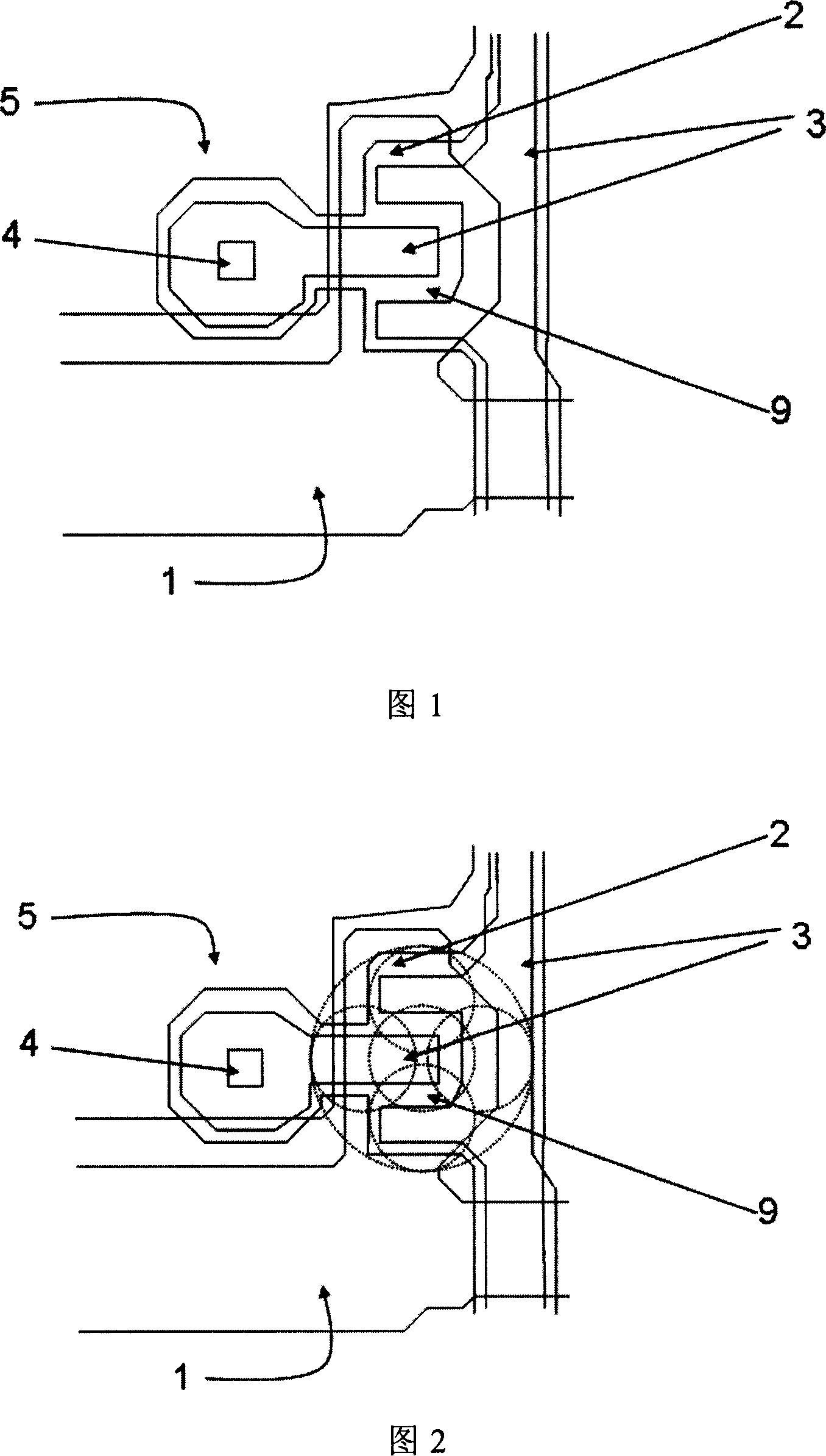
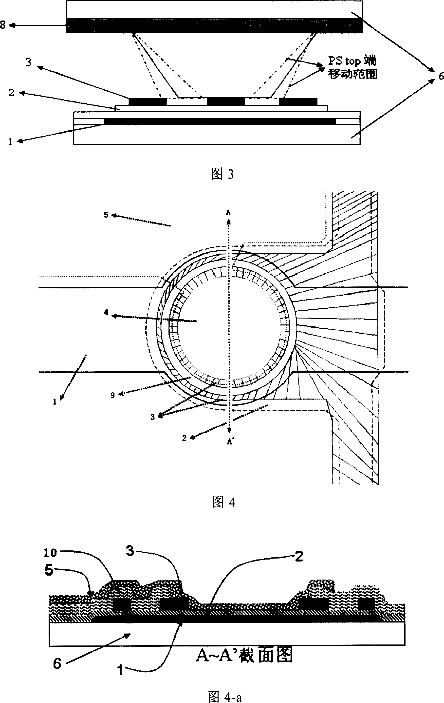
[0025] As shown in Figure 4 and Figure 4A. First, gate leads are formed on the glass substrate 6, wherein the gate electrode 1 and the gate leads are integrated, the gate electrode 1 is circular, and the active layer 2 with a circular structure is formed on the gate electrode 1 by photolithography and other processes. A double circular source-drain electrode 3 is formed on the active layer 2, a circular conductive channel 9 is formed between the source-drain electrodes 3; a passivation layer 10 is formed above the source-drain electrode 3 and the conductive channel 9 On the passivation layer 10, a circular via hole 4 is formed in the source contact, and the pixel electrode 5 is connected to the source terminal of the source-drain electrode 3 through the circular via hole 4. After the final pixel electrode 5 process is completed, a The middle part is a planar device structure.

[0026] Through the design of the circular TFT structure in Figure 4 and Figure 4A, the width-to-len...

Embodiment 2

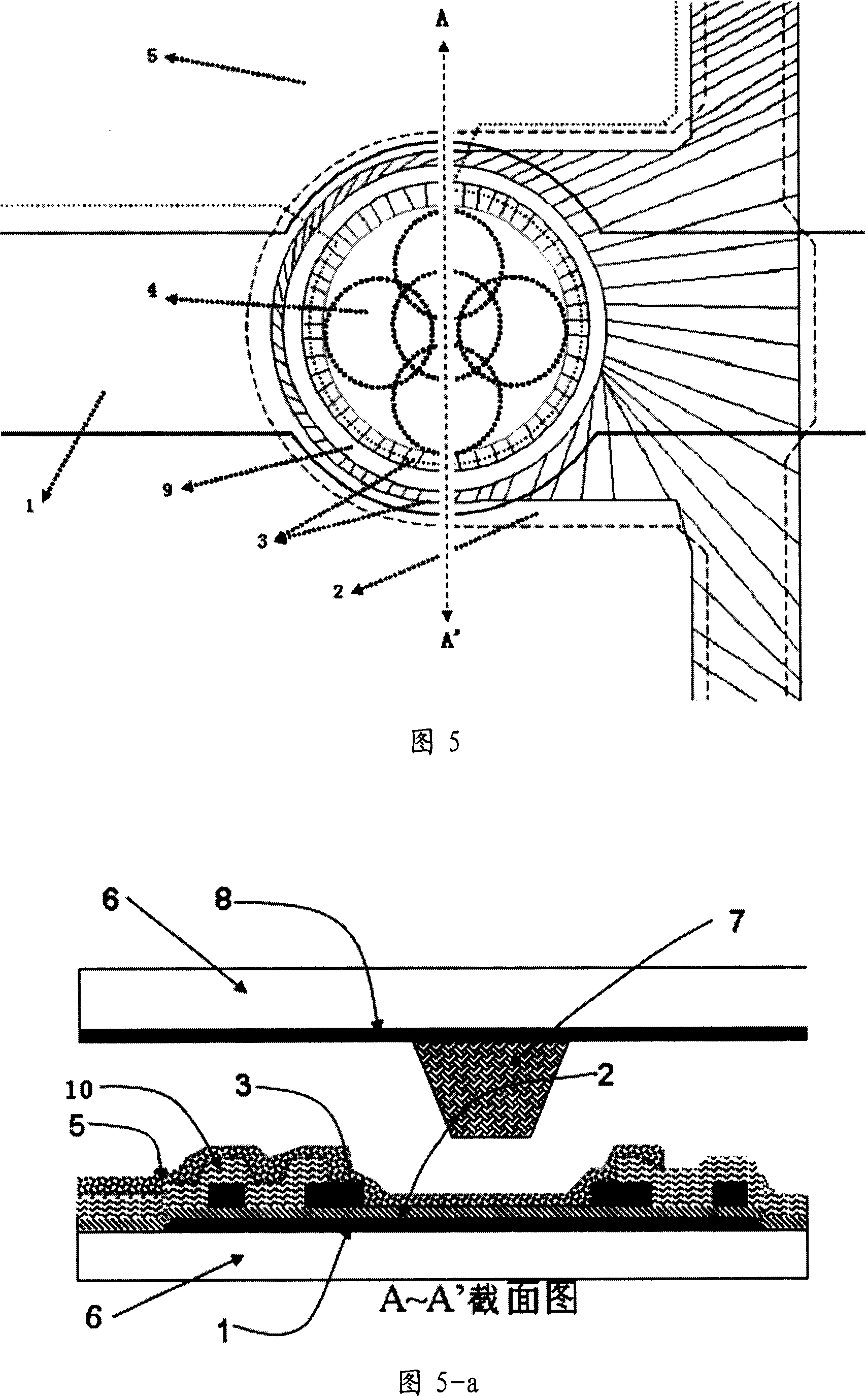
[0031] As shown in Figure 6 and Figure 6A. In consideration of reducing the parasitic capacitance, a hollow structure can be formed on the bottom gate electrode 1 of the TFT device structure described in Embodiment 1, so as to reduce the parasitic capacitance between the gate and the source, and at the same time increase the depth of the annular valley and strengthen the Restriction on the movement of the columnar spacer 7. Wherein, the shape of the hollow structure is preferably circular, and may also be polygonal, and fits with the upper end of the columnar spacer 7 .

Embodiment 3

[0033] As shown in Figure 7 and Figure 7A. In order to avoid disconnection of the pixel electrode 5 due to the step effect formed by the source-drain electrode 3 and the passivation layer 10 at the connection part between the pixel electrode 5 and the via hole 4, it can be used in the TFT device described in Embodiment 1 or Embodiment 2 , on the basis of sacrificing the width-to-length ratio of the part, the source and drain electrodes 3 are circularly opened to form a flat contact surface.


PUM


Abstract

A TFT LCD pixel construction is disclosed, the ring or polygonal TFT component is designed to gate, the via hole part of the pixel is also designed to the gate, the design can increase the W/L of the channel in condition of non-reducing the opening ratio, and increase the on-state current (Ion), the most important is it can limit the post stool (PS) adopted by current color filter.

Description

technical field [0001] The invention belongs to the aspect of TFT LCD pixel structure design, and mainly relates to the design of TFT device structure. Background technique [0002] Most of the currently used TFT LCD pixel structures adopt the structural design shown in Figure 1: [0003] The pixel electrode (ITO) of the TFT is connected to the source (source) through a via hole, and the via hole part is not designed on the gate lead (gate). therefore: [0004] 1. The design of this pixel structure needs to balance the relationship between the two opposing factors of the aperture ratio and whether the pixel is fully charged. In the design of large-scale devices, it is hoped to increase the width-to-length ratio (W / L) to better meet the charging rate requirements. This will increase the width of the conductive channel (channel), increase the size of the TFT, and reduce the The aperture ratio of the device. [0005] 2. This kind of structural design is more complicated, an...

Claims


Application Information

Patent Timeline
Patent Type & Authority Applications(China)
IPC IPC(8): G02F1/1368
Inventor 高文宝
Owner BOE TECH GRP CO LTD
Why Eureka
Try Eureka