Encapsulation structure of optical sensor

A packaging structure and light sensor technology, which is applied to electric solid devices, semiconductor devices, radiation control devices, etc., can solve the problem of colloid layer contaminating metal balls and light sensing areas, avoid contamination of light sensing areas, and reduce packaging. area effect

Inactive Publication Date: 2007-05-30
SIGURD MICROELECTRONICS CORP
View PDF0 Cites 14 Cited by
  • Summary
  • Abstract
  • Description
  • Claims
  • Application Information

AI Technical Summary

Problems solved by technology

[0006] The main purpose of the present invention is to provide a light sensor packaging structure, which is a light sensor exhibiting a CIS package structure, which can solve the problem of col...

Method used


Image

  • Encapsulation structure of optical sensor
  • Encapsulation structure of optical sensor
  • Encapsulation structure of optical sensor

Examples


Embodiment Construction

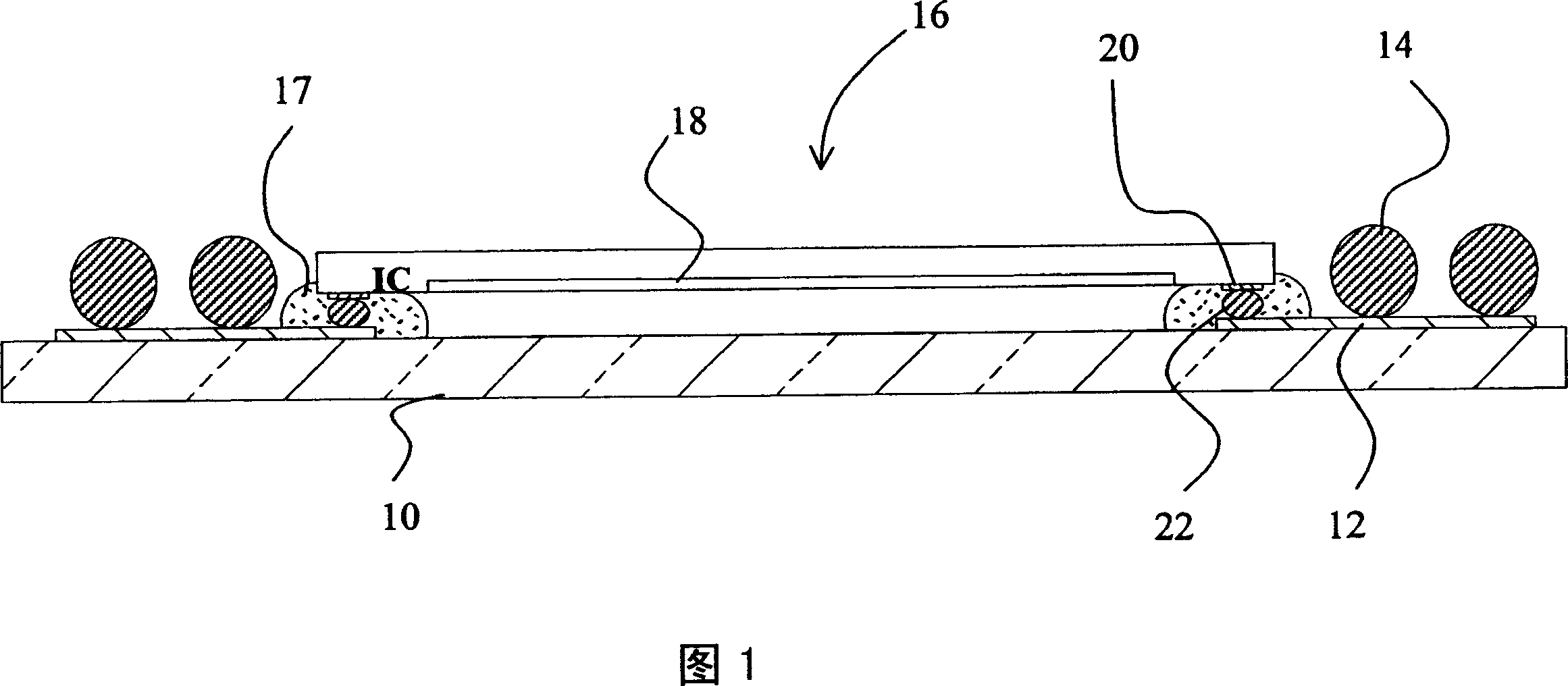
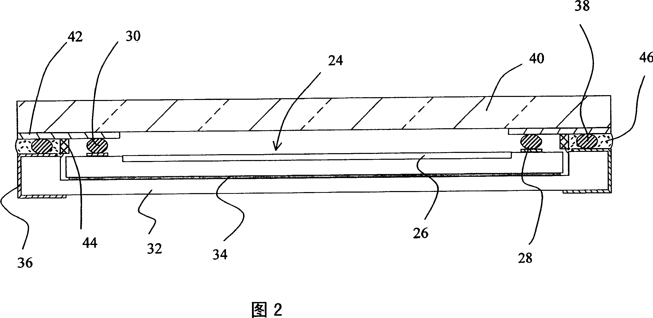
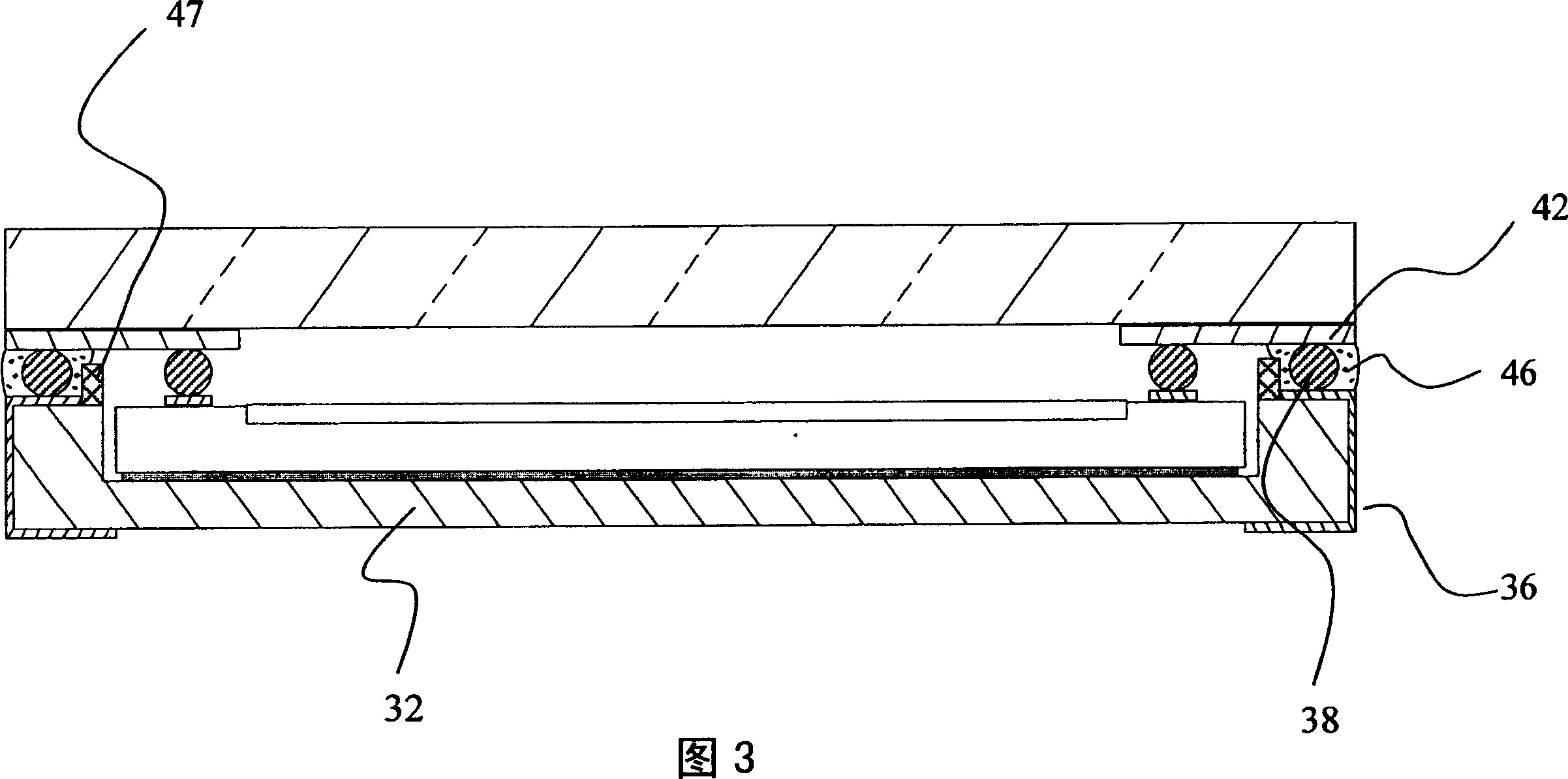
[0033] The present invention relates to a light sensor packaging structure. Please refer to FIG. 2, which is a schematic diagram of an embodiment of the present invention. The present invention mainly includes a light sensing component 24, which includes a light sensing area 26 and a plurality of welding pads 28. There are a plurality of metal connection points 30 on the welding pad 28; a substrate 32, which has an adhesive layer 34 for bonding the light sensing component 24 on the substrate 32, and the edge side of the substrate 32 is provided with metal wiring 36 and A plurality of metal connection points 38 located on the metal wiring 36, a light-transmitting layer 40 covering the light-sensing component 24 and the substrate 32, which can be a light-transmitting glass that can filter a certain wavelength, the light-transmitting layer 40 is provided with metal wiring 42, and metal connection point 30, metal wiring 42, metal connection point 38 form electrical connection with ...


PUM


Abstract

This invention relates to one light sensor sealing structure by use of metal distribution and adhesive layer baseboard to fix the sensor onto baseboard and to change electricity path of sealing structure from COG process into CIS process to improve electricity rate, wherein, it forms gap wall to block glue overflow in proper position to avoid pollution by overflow and metal ball. This invention can reduce sealing area to improve good rate and quality.

Description

technical field [0001] The present invention relates to a light sensor package structure, in particular to a light sensor CIS package structure. Background technique [0002] With the prevalence of audio-visual multimedia, image digitization has become an inevitable trend. The launch of digital cameras, digital video cameras and image scanners and other products represents the advent of the digital image era, and CMOS is one of the important technologies that determine this digital age. The quality, cost, and humanization of its products are the key to the success or failure of an enterprise in this competition. [0003] Please refer to FIG. 1, which is a COG packaging structure of an existing CMOS photosensor (CMOS image sensor). Metal balls (solder balls) 14 for forming electrical connections with metal wiring 12; an optical sensing component 16, which includes a photo-sensing region (sensing region) 18, a plurality of welding pads 20 (pads), on which A plurality of meta...

Claims


Application Information

Patent Timeline
IPC IPC(8): H01L27/146H01L23/488H01L23/31
CPCH01L2224/73253
Inventor 陈柏宏陈懋荣
Owner SIGURD MICROELECTRONICS CORP
Why Eureka
Try Eureka