Method for producing a planar spacer, an associated bipolar transistor and an associated BiCMOS circuit arrangement

A technology of bipolar transistors and spacers, applied in circuits, semiconductor/solid-state device manufacturing, electrical components, etc., to achieve cost-effective and improved electrical characteristics

Inactive Publication Date: 2007-06-06
INFINEON TECH AG
View PDF0 Cites 0 Cited by
  • Summary
  • Abstract
  • Description
  • Claims
  • Application Information

AI Technical Summary

Problems solved by technology

Since the result of this process is not self-adjusting, all fluctuations and tolerances of photolithography are included

Method used


Image

  • Method for producing a planar spacer, an associated bipolar transistor and an associated BiCMOS circuit arrangement
  • Method for producing a planar spacer, an associated bipolar transistor and an associated BiCMOS circuit arrangement
  • Method for producing a planar spacer, an associated bipolar transistor and an associated BiCMOS circuit arrangement

Examples


Embodiment Construction

[0023] The following diagrammatic description illustrates the concept of producing a planar spacer according to the present invention, especially when a planar spacer is used in bipolar transistors and related BiCMOS circuit devices.

[0024] In particular, the sacrificial mask is used as implant hardmask and foundation, so that planar spacers can be formed in a self-adjusting manner to connect multiple regions with one region as close as possible, which will be later Explain, for example, the intrinsic base of a single-multiple bipolar transistor.

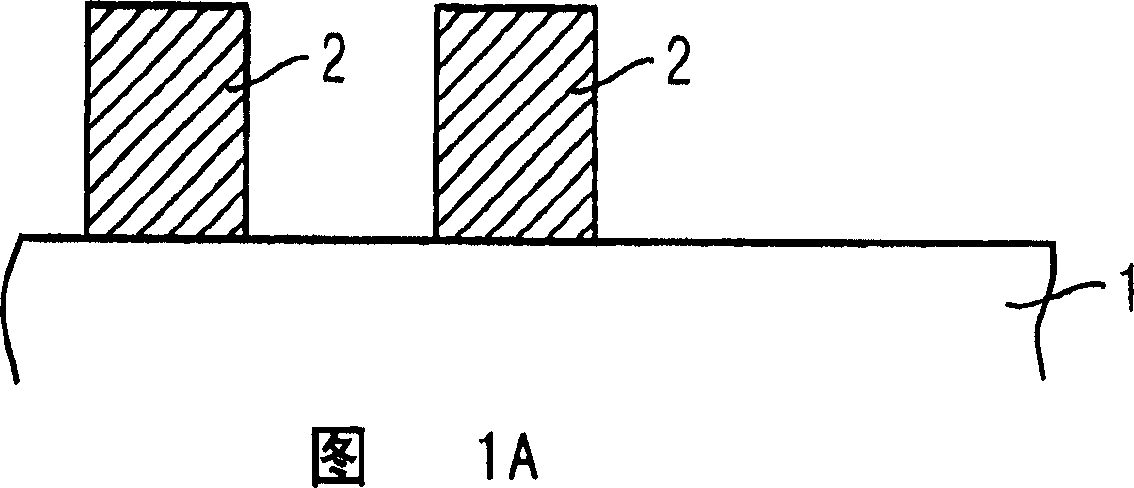
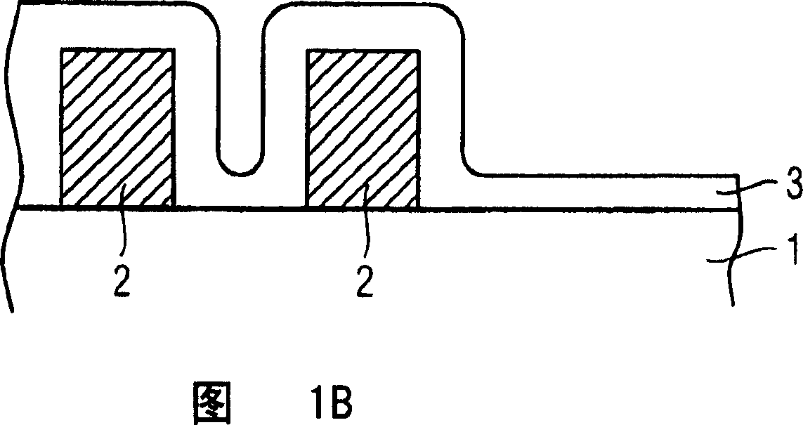
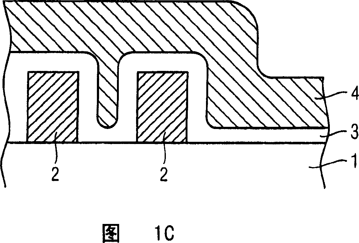
[0025] First, a method of producing a planar spacer, particularly a method of producing a planar outer spacer according to the present invention will be described with reference to FIGS. 1A to 1F. Hereinafter, the term "planar outer spacer" means a substantially flat planar spacer formed on the sidewall of the mask pillar.

[0026] As shown in Figure 1A, firstly a sacrificial mask 2 is formed on the mounting substrate 1, such as ...


PUM


Abstract

The invention relates to a method for producing a planar spacer, an associated bipolar transistor and an associated biCMOS circuit arrangement, wherein the first and second spacer layers (3, 4) are formed on a substrate (1) after a sacrifice mask (2) is formed and first and second spacer layers (3, 4) are embodied. In order to produce auxiliary spacers (4S) on the second spacer layer (4), a first anisotropic etching process is carried out. Afterwards, a second anisotropic etching process is carried out by means of the auxiliary spacers (4S) for producing a planar spacer (PS), thereby making it possible to freely select the height of the thus produced planar spacer (PS), wherein the planarity thereof very much simplifies the continuation of the process. The inventive method makes it possible to produce components exhibiting improved electric properties.

Description

technical field [0001] The present invention relates to a method of fabricating a planar spacer, to an associated bipolar transistor and to an associated BiCMOS circuit arrangement, and more particularly to a method of fabricating self-regulating single-multiple bipolar transistors with improved electrical characteristics in BiCMOS circuits. Background technique [0002] In bipolar transistors, in order to obtain a high cut-off frequency and reduce radio frequency noise, it must be kept in contact with and connected to the intrinsic base with the lowest possible resistance. This is particularly advantageous with a base connection as short as possible, preferably self-adjusting, and with low resistance. [0003] In the case of so-called "single-multiple bipolar transistors", this base connection region is usually defined photolithographically, that is to say not in a self-regulating manner. For example, photolithographically defined emitter pillar blocks are used as implante...

Claims


Application Information

Patent Timeline
IPC IPC(8): H01L21/8249H01L21/331
CPCH01L21/8249H01L29/66242
Inventor C·达尔A·蒂尔克
Owner INFINEON TECH AG
Why Eureka
Try Eureka