Circuit-board laying-out method

A layout method and circuit board technology, applied in the direction of electrical digital data processing, special data processing applications, instruments, etc., can solve problems such as unable to debug and repair, time-consuming and laborious, and prolonged debugging time

A layout method and circuit board technology, applied in the direction of electrical digital data processing, special data processing applications, instruments, etc., can solve problems such as unable to debug and repair, time-consuming and laborious, and prolonged debugging time

CN1979503AInactive Publication Date: 2007-06-13INVENTEC CORP

Image

  • Circuit-board laying-out method
  • Circuit-board laying-out method
  • Circuit-board laying-out method

Examples


Embodiment

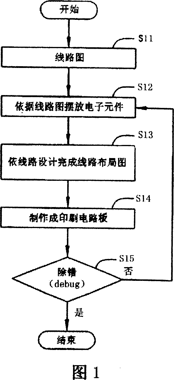
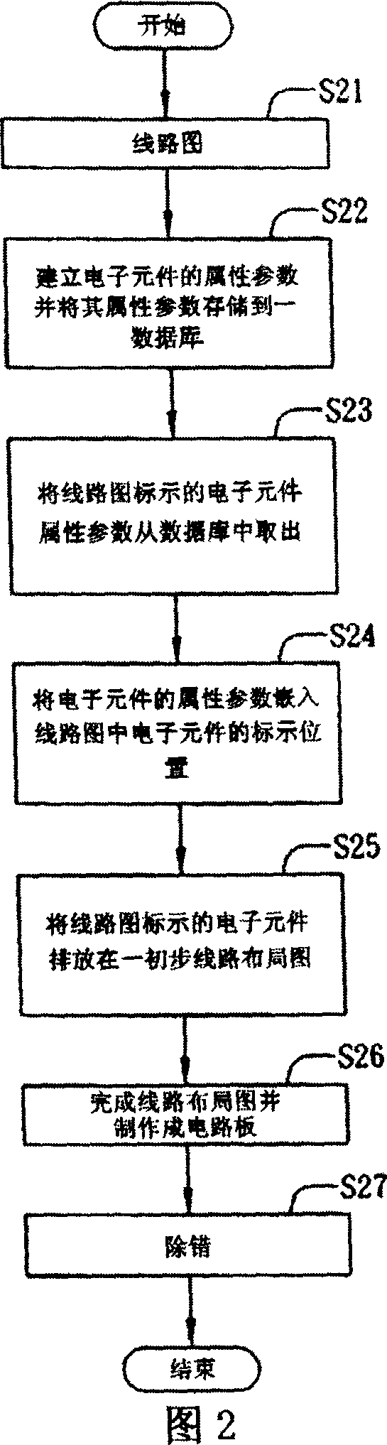
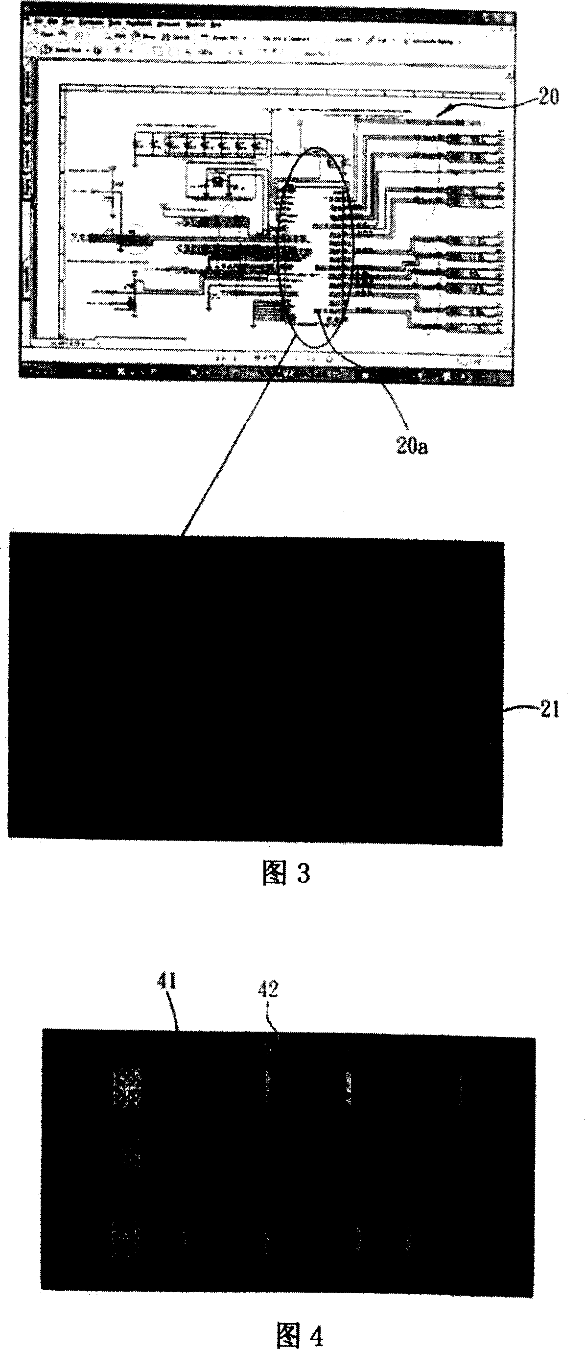
[0020] 2 and 3 at the same time, the circuit board layout method of the present invention includes the following steps. As shown in step S21, a circuit diagram 20 is first provided; then, in step S22, the circuit board layout method according to the electronic component 20a in the circuit diagram 20 is established. Attribute parameters, and store the electronic component 20a and its attribute parameters 21 in a database. The electronic component 20a is a chipset, a central processing unit, a driver chip, a control chip, a special application chip or a passive component. The passive component is Resistors, capacitors, inductors or switches; then in step S23, the attribute parameters 21 of the electronic component 20a marked in the circuit diagram 20 are retrieved from the database; then, as shown in step S24, the electronic component 20a in the circuit diagram 20 The attribute parameter 21 is embedded in the position marked by the electronic component 20a in the circuit diagram 20,...


PUM


Abstract

The invention is a circuit board layout method, comprising the steps of: providing a circuit diagram; establishing and storing electronic components and their attribute parameters in a database; drawing the attribute parameters the circuit diagram indicates from the database and inserting the attribute parameters of electronic components in the circuit diagram in the indication positions of the circuit diagram; when converting a circuit diagram into a circuit layout diagram, a designer obtains sizes, pin positions and connection relations of electronic components and other graphic data at the time of circuit layout design according to the attribute parameters of electronic components in the circuit diagram. And the invention benefits circuit layout design, raising layout efficiency and reducing artificial mistakes.

Description

Technical field [0001] The present invention relates to a circuit board layout method, in particular to a method of embedding graphic attribute parameters in an electronic component of a circuit diagram to meet the requirements of circuit layout. Background technique [0002] For electronic devices with excellent performance, in addition to selecting high-quality electronic components and reasonable circuits, the layout of printed circuit board components and the impedance of circuit connections are also factors that affect the quality of the electronic device; for circuits with the same components and parameters Because of different component layout designs and circuit connections, there will be different impedance values, and the impedance magnitude affects signal transmission and control stability. Therefore, how to reduce the impedance generated by the circuit layout and eliminate the noise interference caused by improper wiring, which is conducive to the installation, debugg...

Claims


Application Information

Patent Timeline
13 Jun 2007
Publication
CN1979503A
IPC
G06F17/50
Inventors
伍靖; 杨淑敏