Nanoshape patterning techniques that allow high-speed and low-cost fabrication of nanoshape structures

Active Publication Date: 2018-07-17
BOARD OF RGT THE UNIV OF TEXAS SYST
View PDF24 Cites 46 Cited by
  • Summary
  • Abstract
  • Description
  • Claims
  • Application Information

AI Technical Summary

Problems solved by technology

Furthermore, the method comprises etching an underlying sacrificial polymeric layer following the etching of the polymeric residual layer, wherein the underlying sacrificial polymeric layer etch results in an undercut.

Method used


Image

  • Nanoshape patterning techniques that allow high-speed and low-cost fabrication of nanoshape structures
  • Nanoshape patterning techniques that allow high-speed and low-cost fabrication of nanoshape structures
  • Nanoshape patterning techniques that allow high-speed and low-cost fabrication of nanoshape structures

Examples


Embodiment Construction

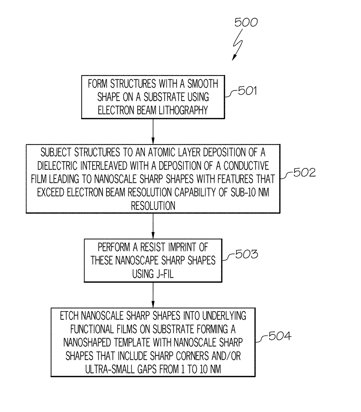
[0055]The present invention focuses on using imprint lithography to pattern nanoscale shapes. An exemplary imprint lithography technique, known as Jet and Flash Imprint Lithography (J-FIL) is described next. A unique feature of J-FIL is that it uses a targeted resist dispense approach that allows adaptive material deposition to match pattern density variations in the mask that is to be replicated. This combined with low viscosity resist formulations leads to high throughput processes. A process for using imprint lithography to pattern nanoscale shapes is discussed below in connection with FIGS. 3 and 4A-4D. FIG. 3 is a flowchart of a method 300 for using imprint lithography to pattern nanoscale shapes in accordance with an embodiment of the present invention. FIG. 3 will be discussed in conjunction with FIGS. 4A-4D, which depict cross-sectional views of patterning nanoscale shapes using the steps described in FIG. 3 in accordance with an embodiment of the present invention.

[0056]Ref...


PUM

PropertyMeasurementUnit
thicknessaaaaaaaaaa
thicknessaaaaaaaaaa
sizeaaaaaaaaaa

Abstract

A method for template fabrication of ultra-precise nanoscale shapes. Structures with a smooth shape (e.g., circular cross-section pillars) are formed on a substrate using electron beam lithography. The structures are subject to an atomic layer deposition of a dielectric interleaved with a deposition of a conductive film leading to nanoscale sharp shapes with features that exceed electron beam resolution capability of sub-10 nm resolution. A resist imprint of the nanoscale sharp shapes is performed using J-FIL. The nanoscale sharp shapes are etched into underlying functional films on the substrate forming a nansohaped template with nanoscale sharp shapes that include sharp corners and / or ultra-small gaps. In this manner, sharp shapes can be retained at the nanoscale level. Furthermore, in this manner, imprint based shape control for novel shapes beyond elementary nanoscale structures, such as dots and lines, can occur at the nanoscale level.

Description

CROSS REFERENCE TO RELATED APPLICATIONS[0001]This application is related to the following commonly owned U.S. patent application:[0002]Provisional Application Ser. No. 62 / 067,496, “Precise Nanoscale Shape Controlled Large Area Patterning,” filed Oct. 23, 2014, and claims the benefit of its earlier filing date under 35 U.S.C. § 119(e).GOVERNMENT INTERESTS[0003]This invention was made with government support under Grant No. EEC 1160494 and Grant No. ECCS1120823 awarded by the National Science Foundation. The U.S. government has certain rights in the invention.TECHNICAL FIELD[0004]The present invention relates generally to fabrication of nanostructures, and more particularly to nanoshape patterning techniques that allow high-speed and low-cost fabrication of nanoshape structures.BACKGROUND[0005]In a variety of nano-device applications, high-speed (low-cost) fabrication of nanostructures with sharp shapes is important. This includes devices exploiting nanoscale phenomena in optics, magn...

Claims


Application Information

Patent Timeline
Patent Type & Authority Patents(United States)
IPC IPC(8): H01L21/02G03F7/00H01L21/308B81C1/00G11B5/74B82Y40/00H01L29/94
CPCH01L21/02521B81C1/00031G03F7/0002H01L21/02381H01L21/02617H01L21/3086Y10S977/89B82Y40/00G11B5/746H01L29/945Y10S977/887Y10S977/888B81C2201/0187G02B6/1226
Inventor SREENIVASAN, SIDLGATA V.CHERALA, ANSHUMANCHOPRA, MEGHALIBONNECAZE, ROGERABED, OVADIAYIN, BAILEYMALLAVARAPU, AKHILASINGHAL, SHRAWANGAWLIK, BRIAN
Owner BOARD OF RGT THE UNIV OF TEXAS SYST
Why Eureka
Try Eureka