
Wafer dividing method

a technology of dividing method and wafer, which is applied in the direction of electrical apparatus, semiconductor devices, semiconductor/solid-state device details, etc., can solve the problems of limiting the number of devices which can be arranged on the wafer, reducing the efficiency of laser grooving process, and reducing the number of devices. the effect of a single, low cost and time-saving

Active Publication Date: 2018-07-24
DISCO CORP
View PDF48 Cites 1 Cited by
  • Summary
  • Abstract
  • Description
  • Claims
  • Application Information

AI Technical Summary

Benefits of technology

The present invention provides a cost-effective and efficient method for dividing a wafer into smaller dies while reducing the risk of damage to the wafer. This is achieved by a method that meets the technical features outlined in the patent claim. Preferred embodiments of the invention are outlined in the dependent claims.

Problems solved by technology

This requirement of a relatively large laser groove width results in a wider spacing between neighbouring devices and thus limits the number of devices which can be arranged on the wafer, i.e., the packing density.
Further, multiple laser passes are necessary to provide such a wide laser groove, thereby rendering the laser grooving process time-consuming and inefficient.
Moreover, due to the heat generated in the laser grooving process, the remainder of the surface layer, such as the low-k layer, formed on the front side of the wafer may at least partly delaminate, causing damage to the devices and / or the wafer substrate.
Such damage may not only affect the functionality of the devices but also reduce the die strength of the resulting device chips.

Method used


Image

  • Wafer dividing method
  • Wafer dividing method
  • Wafer dividing method

Examples


first embodiment

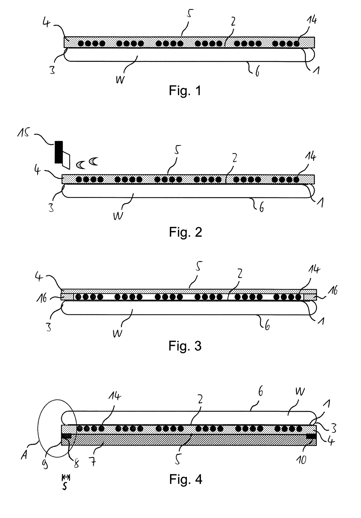
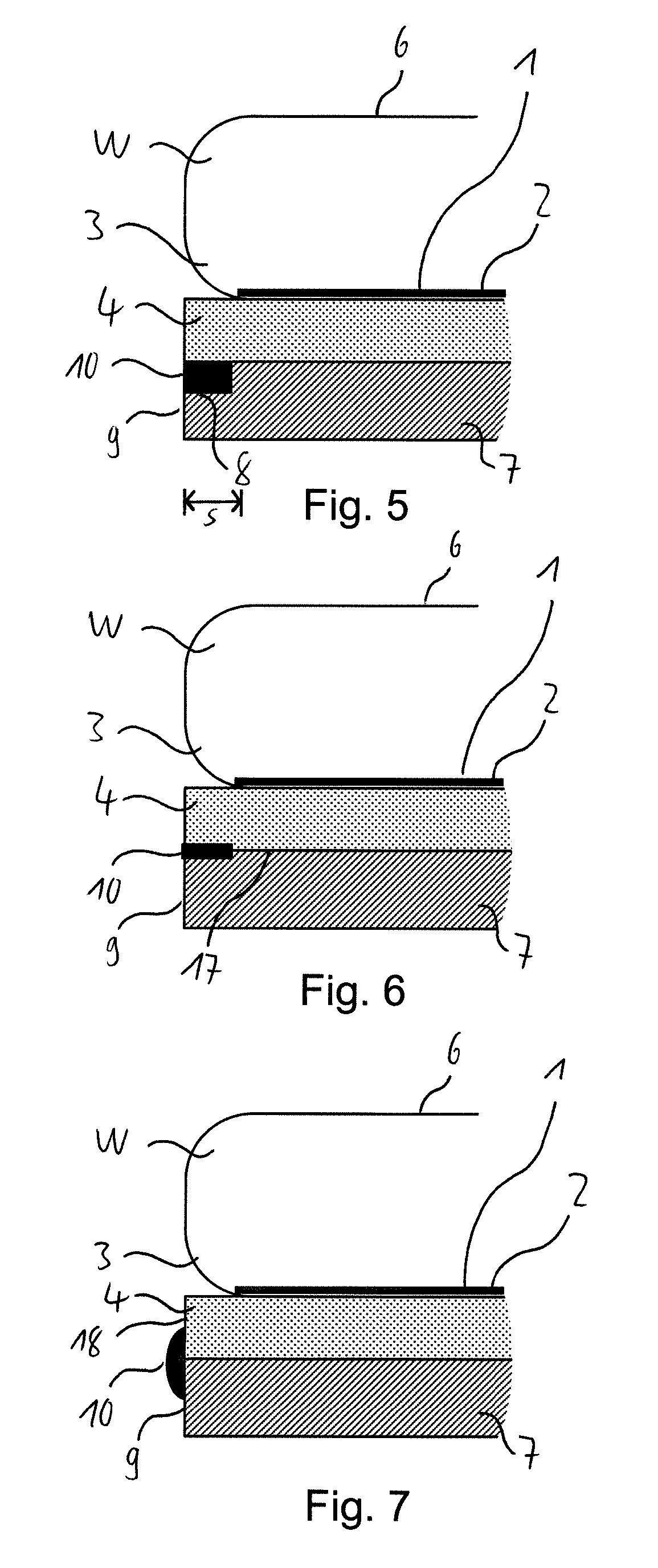
[0101]In the following, a method of dividing a wafer W according to the present invention will be described with reference to FIGS. 1 to 13.

[0102]FIG. 1 depicts the outcome of a first step of the method of dividing a wafer according to the first embodiment of the present invention. In this first step, an adhesive tape 4 is attached to the pattern side 1 of the wafer W. In other words, the pattern side 1 is laminated with the adhesive tape 4. The adhesive tape 4 preferably has the same shape as the wafer W and is attached thereto concentrically. When attached to the wafer W, the adhesive tape 4 adheres to the devices formed in the device area 2 of the pattern side 1.

[0103]The adhesive tape 4 allows for protection of the devices formed in the device area 2 of wafer W.

[0104]The adhesive of the adhesive tape 4 on the side thereof facing the pattern side 1 of the wafer W may be curable by an external stimulus, such as heat, UV radiation, an electric field and / or a chemical agent. In this...

second embodiment

[0140]Specifically, as is shown in FIG. 14, in the method of the second embodiment, the cutting of the wafer W is performed in seventh and eighth steps prior to the application of the protective layer 20.

[0141]Subsequently, as is schematically shown in FIG. 15, a liquid mold material for the protective layer is applied to the backside of the wafer W in a ninth step. The liquid mold material penetrates into the cuts 22 between the dies 23 created in the cutting process. Hence, the protective layer 20 can be reliably applied also to the side surfaces of the dies 23, thus providing particularly reliable protection.

[0142]The liquid mold material is curable by an external stimulus, such as heat, UV radiation, an electric field and / or a chemical agent. After the liquid mold material for the protective layer 20 has been applied to the backside of the wafer W, it is cured by applying the external stimulus thereto, e.g., by heating in an oven for the case of a heat curable, e.g., thermosetti...

third embodiment

[0153]In a thirteenth step of the third embodiment, the result of which is shown in FIG. 20, the carrier 7 and the adhesive tape 4 are removed from the wafer W. In particular, the adhesive of the adhesive tape 4 on the side thereof facing the pattern side 1 of the wafer W may be cured by applying an external stimulus thereto, as has been detailed above, so as to lower the adhesive force of the adhesive, thus allowing for an easy removal of the adhesive tape 4 and the carrier 7 from the wafer W.

[0154]Subsequently, the individual separated dies 23 can be picked up from the adhesive pick-up tape 24 by a pick-up device in the same manner as for the first and second embodiments. The spacing between the individual dies 23 can be increased by radially stretching the pick-up tape 24 in order to facilitate the pick-up process.


PUM


Abstract

A wafer having on one side a device area with devices partitioned by division lines is divided into dies. An adhesive tape for protecting the devices is attached to the one side of the wafer, and a carrier for supporting the adhesive tape is attached to the outside of the adhesive tape. The other side of the wafer is ground to adjust the wafer thickness, and a protective layer is applied to the ground side of the wafer. The side of the wafer opposite to the adhesive tape is mechanically partially cut along the division lines with a first cutting width. A remaining part of the wafer, in the thickness direction thereof in the region or regions where the partial cut or cuts had been formed, is cut with a second cutting width. The second cutting width is smaller than or equal to the first cutting width.

Description

TECHNICAL FIELD[0001]The present invention relates to a method of dividing a wafer, such as a semiconductor wafer, having on one side a device area with a plurality of devices partitioned by a plurality of division lines, into dies.TECHNICAL BACKGROUND[0002]In a semiconductor device fabrication process, a wafer having a device area with a plurality of devices partitioned by a plurality of division lines is divided into individual dies. This fabrication process generally comprises a grinding step for adjusting the wafer thickness and a cutting step of cutting the wafer along the division lines to obtain the individual dies. In order to protect the devices formed on the wafer during this fabrication process and to suitably position the individual dies, an adhesive tape can be attached to the side of the wafer having the devices formed. thereon.[0003]In known semiconductor device fabrication processes, such as flip chip packaging, Wafer Level Chip Scale Package (WLCSP) and Embedded Waf...

Claims


Application Information

Patent Timeline
Patent Type & Authority Patents(United States)
IPC IPC(8): H01L21/78H01L21/268H01L21/3065H01L21/56H01L23/00H01L21/683H01L23/544H01L23/31
CPCH01L21/78H01L21/268H01L21/3065H01L21/561H01L21/6835H01L21/6836H01L24/92H01L2924/35121H01L2224/94H01L2224/92H01L2223/54486H01L2221/68381H01L2221/68327H01L2221/68318H01L2221/6834H01L21/568H01L23/3114H01L23/544H01L24/94H01L2224/11H01L2221/68304H01L21/304H01L21/56H01L21/30
Inventor PRIEWASSER, KARL HEINZ
Owner DISCO CORP
Learn More