Method of producing an optical sensor at wafer-level and optical sensor
- Summary
- Abstract
- Description
- Claims
- Application Information
AI Technical Summary
Benefits of technology
Problems solved by technology
Method used
Image
Examples
Embodiment Construction
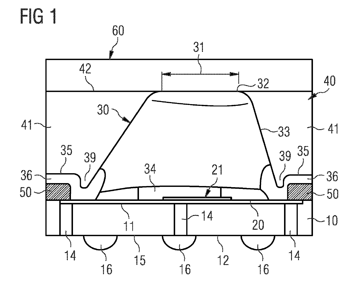
[0046]FIG. 1 shows an exemplary embodiment of an optical sensor. The drawing depicts a cross-section of an optical sensor comprising a semiconductor substrate (as part of a wafer 10), an integrated circuit 20, a first mold structure 30, and a second mold structure 40.
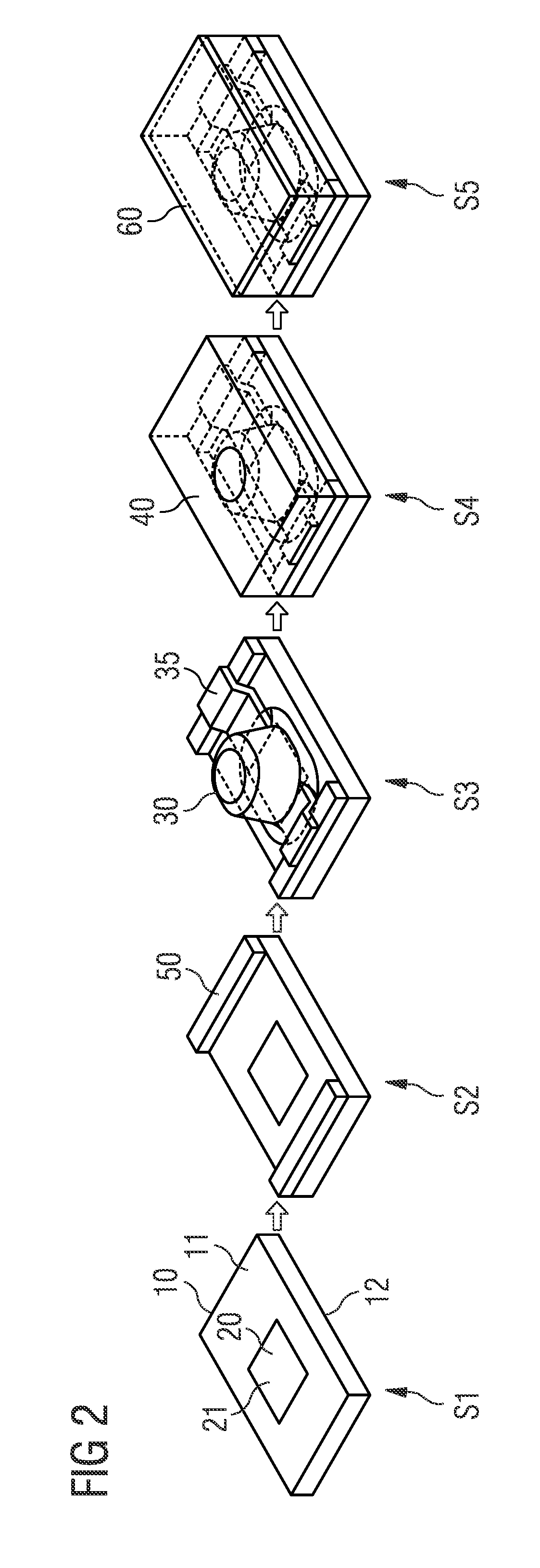
[0047]The optical sensor has been manufactured at wafer-level together will a plurality of other sensors as will be discussed in greater detail below. In a final step, however, the wafer carrying a plurality of optical sensors has been singulated into final optical sensor package such as the one shown in FIG. 1.
[0048]The substrate (as part of wafer 10) comprises several through silicon vias 14 electrically connecting a front surface 11 and a back surface 12. A redistribution layer 15 and a number of solder balls (bumps) 16 are located on the back surface 12. The integrated circuit 20 is integrated into the substrate on the front surface 11 and comprises a light sensitive component 21. Furthermore, the integrated circuit...
PUM
 Abstract
Description
Claims
Application Information


