
Partially asynchronous clock scheme for SAR ADC

a synchronous clock and adc technology, applied in the field of electrical circuitry for data conversion, can solve the problems of reducing the overall speed of data conversion operations, difficult to optimize the time of compare vs dac settling without duty cycle adjustments or higher frequency clocks, and designing this delay adds power and complexity

Active Publication Date: 2018-08-14
NXP USA INC
View PDF18 Cites 18 Cited by
  • Summary
  • Abstract
  • Description
  • Claims
  • Application Information

AI Technical Summary

Benefits of technology

The present invention is about improving the design of analog-to-digital converters (ADCs) by using a partially asynchronous clocking scheme in an SAR ADC. This allows for faster data conversion without requiring additional analog delay circuitry. The invention uses a synchronous input clock to initiate the compare phase and an asynchronous, self-generated clock edge to end the compare phase, thereby adjustably controlling the settling and comparison timing during each successive approximation phase while maintaining a fixed period for the "compare time plus DAC settling time." This results in faster conversion speeds without sacrificing performance demands for the worst case scenario. The invention also includes a disclosed synchronous ADC input clock edge that initiates each compare phase and an asynchronous, self-generated clock edge that ends each compare phase and begins the DAC settling phase to begin the next bit approximation. Overall, the invention provides a more efficient and effective solution for designing high-speed analog-to-digital converters.

Problems solved by technology

For example, fully synchronous SAR ADCs typically require an over-sampling clock that is a multiple of the ADC sample frequency, and are designed on the basis of a fixed DAC settling time and fixed compare times, in which case the clock frequency must be chosen to meet the worst case combination of those delays, thereby reducing the overall speed of data conversion operations.
And with fully synchronous SAR ADCs, it is also difficult to optimize for compare vs DAC settling time without duty cycle adjustments or higher frequency clocks.
In contrast, fully asynchronous SAR ADCs are much faster and do not require a fast input clock, but there are design complexities and performance drawbacks for asynchronous ADCs which typically require that an analog delay be generated in order to match the worst case DAC settling time.
Designing this delay adds power and complexity and likely requires some trimming / calibration.
In addition, the difficulty in knowing the end of the conversion time with asynchronous converters typically requires that the input clock rate be chosen for worst case approximation times, thereby sacrificing some of the speed performance advantages that would otherwise accrue for a fully asynchronous SAR ADC.
As seen from the foregoing, the existing SAR ADC solutions for quickly and efficiently performing analog-to-digital conversions are extremely difficult at a practical level by virtue of the difficulty balancing the design constraints for providing an efficient, low complexity SAR ADC with the performance demands for performing high speed analog-to-digital conversion.

Method used


Image

  • Partially asynchronous clock scheme for SAR ADC
  • Partially asynchronous clock scheme for SAR ADC
  • Partially asynchronous clock scheme for SAR ADC

Examples


Embodiment Construction

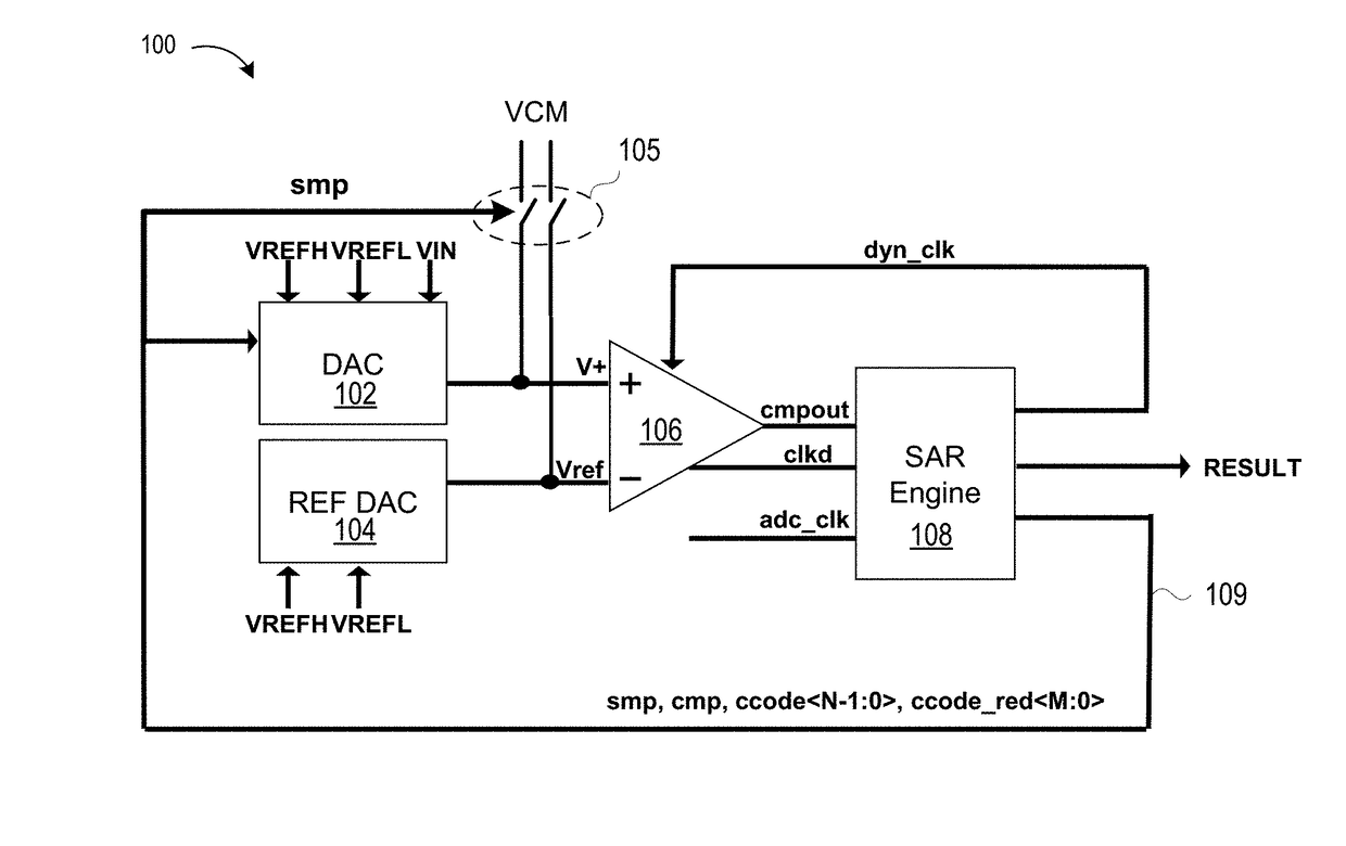
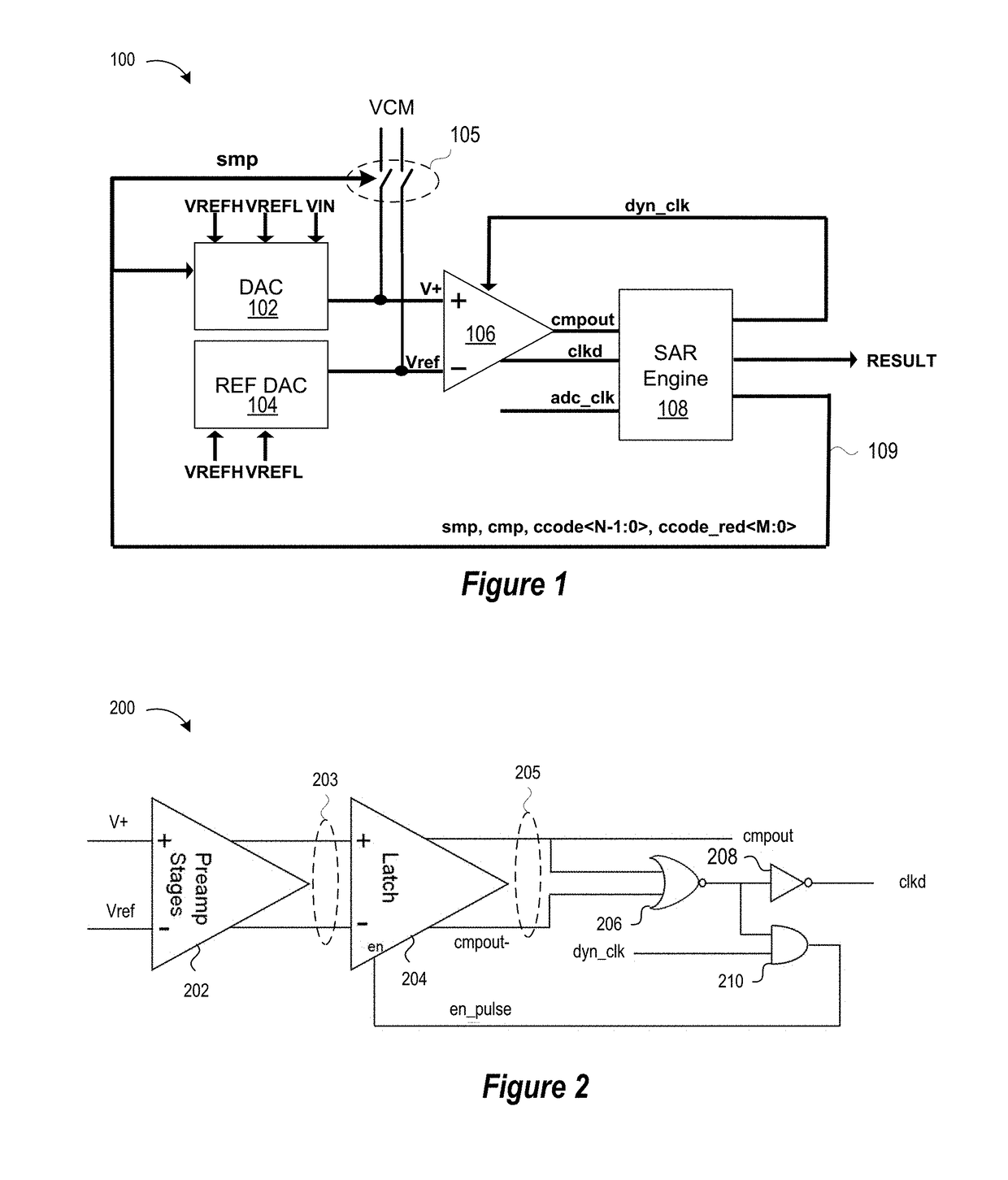
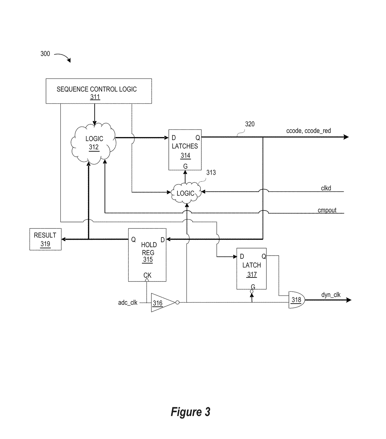
[0014]A system, apparatus, and methodology are described for providing a partially asynchronous clocking scheme in an SAR ADC which uses asynchronous compare times within a fixed period for the “compare time plus DAC settling time” to increase the ADC conversion speed without requiring analog delay circuitry. In selected embodiments, the asynchronous compare times are controlled with a clocking scheme which uses a synchronous comparator input clock (e.g., dyn_clk) to end the settling time and initiate the compare timing and uses asynchronous self-generated clock edges (e.g., clkd) to end the compare timing and begin the settling time of the next bit, thereby adjustably controlling the settling and comparison timing during each successive approximation phase while maintaining a fixed period for the “compare time plus DAC settling time.” In particular, a disclosed synchronous ADC input clock edge begins each compare phase (and ends the preceding settling phase) and an asynchronous, se...


PUM


Abstract

A method and apparatus are provided for controlling an SAR ADC by generating a first signal to control sampling of an analog input voltage at a DAC, and then generating a second signal to start a successive approximation sequence at a comparator and SAR engine to convert the analog input voltage to an N-bit digital value, where the successive approximation sequence includes a settling phase for each bit of the N-bit digital value and is controlled to synchronously end in response to a first synchronous clock signal, and also includes a comparison phase for each bit of the N-bit digital value to allow for comparison of the analog input voltage to a reference voltage, where each comparison phase is controlled to synchronously start in response to the first synchronous clock signal and asynchronously end in response to a second asynchronous clock signal that is self-generated by the comparator.

Description

BACKGROUND OF THE INVENTION[0001]Field of the Invention[0002]The present invention is directed in general to electrical circuitry for data conversion. In one aspect, the present invention relates generally to analog-to-digital converter (ADC) systems.[0003]Description of the Related Art[0004]In electronics, an analog-to-digital converter (ADC, A / D, or A-to-D) is a system that converts an analog signal into a digital signal. A successive approximation register (SAR) ADC is a type of analog-to-digital converter that converts a continuous analog waveform into a discrete digital representation via a binary search. During this binary search, the ADC makes a decision for each bit of resolution, thus converging upon a digital output for each conversion. SAR ADCs can be designed as fully synchronous, using a fixed time for each bit decision based on an input clock, or asynchronous, having variable time for each bit decision based on a self-timed comparator delay. As will be appreciated, the...

Claims


Application Information

Patent Timeline
Patent Type & Authority Patents(United States)
IPC IPC(8): H03M1/46H03M1/68H03M1/10H03M1/06
CPCH03M1/462H03M1/1061H03M1/0697H03M1/468H03M1/687H03M1/069H03M1/125
Inventor BERENS, MICHAEL T.MAI, KHOI B.BAKER, GEORGE E.
Owner NXP USA INC
Learn More