Scanning method for screening of electronic devices

a technology for electronic devices and screening methods, applied in the direction of resistance/reactance/impedence, measurement devices, instruments, etc., can solve the problems of difficult defect detection in integrated circuits (ics), requiring extensive failure analysis, and identifying defects in ics generally requires extensive failure analysis, so as to improve the effectiveness of psa screening

Active Publication Date: 2018-10-09
NAT TECH & ENG SOLUTIONS OF SANDIA LLC
View PDF17 Cites 12 Cited by
  • Summary
  • Abstract
  • Description
  • Claims
  • Application Information

AI Technical Summary

Benefits of technology

[0008]We have developed a new method for visualizing the spatial distribution of anomalies in devices under test using power spectrum analysis (PSA). Our method can be used to identify the physical locations in a device under test (DUT) that give rise to observable differences in the response of the DUT to PSA stimuli, relative to a standard, expected, or nominal response. These differences can be used, for example, to separate devices believed to be “good”, i.e. properly functioning, from devices suspected to be damaged, or to separate devices believed to be genuine from devices suspected to be counterfeit. The ability to identify specific physical locations as sources of anomalous response will enhance the effectiveness of PSA screening for these and other purposes. In practice, an appropriate disposition can be made of each inspected device based, at least in part, on the spatially resolved information that is obtained.

Problems solved by technology

Defect detection in integrated circuits (ICs), for example, can be challenging because an IC can have millions of transistors with a feature size less than a micrometer.
Therefore, to identify a defect in an IC generally requires extensive failure analysis.
However, these techniques are quite complex, time-consuming, and costly.
Further, an IC or other circuit component can contain a latent defect (also referred to as a “failure precursor”) that is likely to develop into a defect after a period of use.
Reliability testing can be quite time-consuming and can significantly increase the production cost.
However, the selection of any screening technique involves tradeoffs among cost, accuracy, discrimination among different anomalies, destructiveness, and other factors.

Method used


Image

  • Scanning method for screening of electronic devices
  • Scanning method for screening of electronic devices
  • Scanning method for screening of electronic devices

Examples


Embodiment Construction

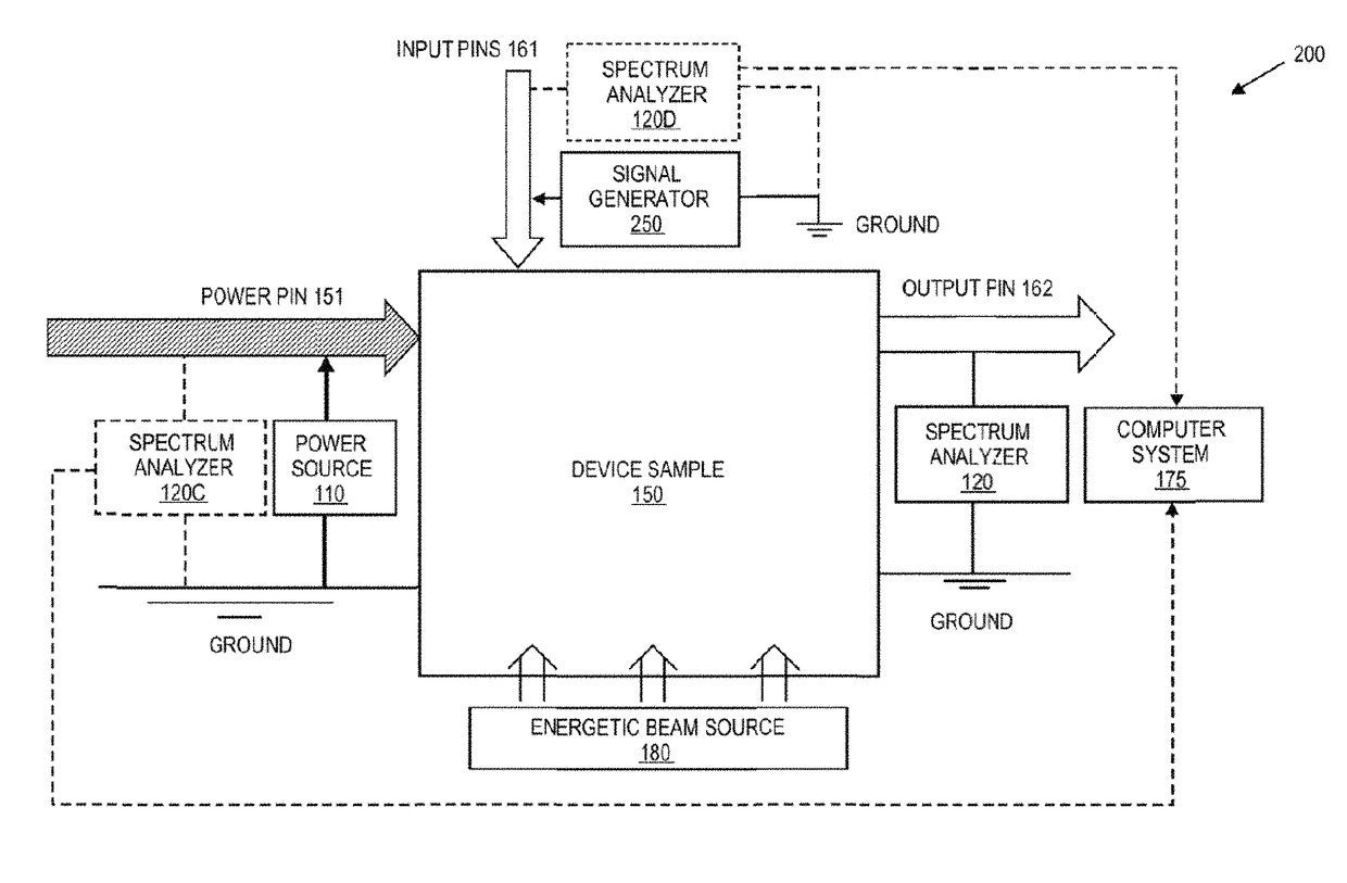
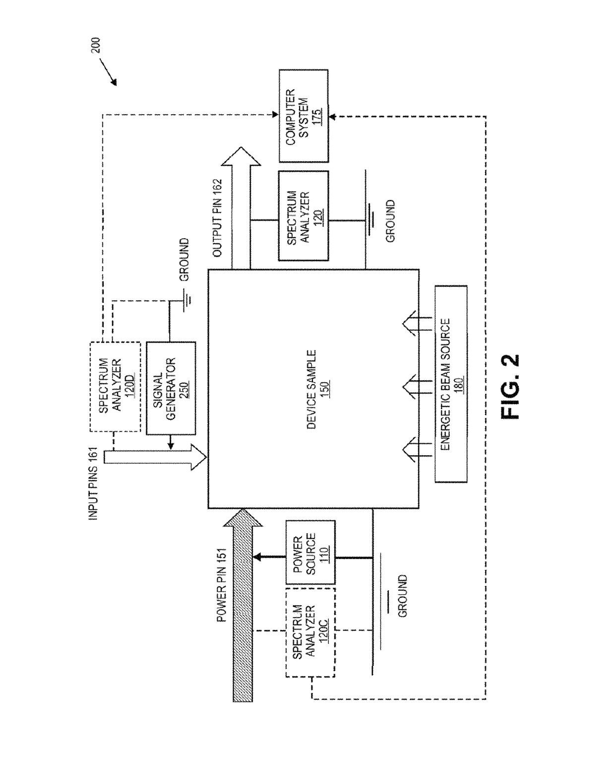
[0033]Power spectrum analysis (PSA) is a technique that indirectly measures the frequency response of a device when the device is subject to a dynamic stimulus. Devices with defects tend to exhibit frequency responses that differ from the frequency responses of healthy devices, i.e. devices that are fully functional and meet all desired manufacturing tolerances.

[0034]Conventional techniques of failure analysis are effective only when defects give rise to an observable electrical signature of a failure. However, these signatures, and especially the signatures of latent defects, can be masked by the background electrical signals of normal operation. One advantage of PSA is that it can be more effective than conventional methods in detecting masked indications of failure or other anomalous behavior.

[0035]FIG. 1 is a block diagram of an example system 100 for power spectrum analysis (PSA). The system 100 includes a power source 110 coupled between a power pin 151 and the ground of a sam...


PUM


Abstract

A visualization method for screening electronic devices is provided. In accordance with the disclosed method, a probe is applied to a grid of multiple points on the circuit, and an output produced by the circuit in response to the stimulus waveform is monitored for each of multiple grid points where the probe is applied. A power spectrum analysis (PSA) produces a power spectrum amplitude, in each of one or more frequency bins, on the monitored output for each of the multiple grid points. The PSA provides a respective pixel value for each of the multiple grid points. An image is displayed, in which image portions representing the multiple grid points are displayed with the respective pixel values.

Description

CROSS-REFERENCE TO RELATED APPLICATIONS[0001]This application is a continuation-in-part of U.S. patent application Ser. No. 14 / 882,710, which is a continuation-in-part of U.S. patent application Ser. No. 13 / 309,281. Application Ser. No. 14 / 882,710, which is commonly owned herewith, was filed on Oct. 14, 2015 by P. Tangyunyong et al. under the title “Defect Screening Method for Electronic Circuits and Circuit Components Using Power Spectrum Analysis”. The entirety thereof is hereby incorporated herein by reference. Application Ser. No. 13 / 309,281, which is commonly owned herewith, was filed on Dec. 1, 2011 by P. Tangyunyong under the title “Power Spectrum Analysis for Defect Screening in Integrated Circuit Devices” and issued on Nov. 17, 2015 as U.S. Pat. No. 9,188,622. The entirety thereof is hereby incorporated herein by reference.FEDERALLY SPONSORED RESEARCH[0002]The United States Government has rights in this invention pursuant to Department of Energy Contract No. DE-AC04-94AL850...

Claims


Application Information

Patent Timeline
Patent Type & Authority Patents(United States)
IPC IPC(8): G01R31/307G01R31/311G01R31/303G01R27/28
CPCG01R31/307G01R27/28G01R31/303G01R31/311G01R23/18G01R31/2879
Inventor TANGYUNYONG, PAIBOONCOLE, JR., EDWARD I.LOUBRIEL, GUILLERMO M.BEUTLER, JOSHUA
Owner NAT TECH & ENG SOLUTIONS OF SANDIA LLC
Why Eureka
Try Eureka